Present Address: ]Low Temperature Laboratory, Department of Applied Physics, Aalto University School of Science, POB 13500, FI-00076 AALTO, Finland
Hybrid rf SQUID qubit based on high kinetic inductance
Abstract
We report development and microwave characterization of rf SQUID (Superconducting QUantum Interference Device) qubits, consisting of an aluminium-based Josephson junction embedded in a superconducting loop patterned from a thin film of TiN with high kinetic inductance. Here we demonstrate that the systems can offer small physical size, high anharmonicity, and small scatter of device parameters. The hybrid devices can be utilized as tools to shed further light onto the origin of film dissipation and decoherence in phase-slip nanowire qubits, patterned entirely from disordered superconducting films.
I Introduction
Various applications of superconducting quantum bits (qubits), see for example Refs. devoret13, and barends14, , benefit from building blocks with good reproducibility of device parameters, high anharmonicity of the energy level spacings, and compact physical size. These requirements apply in particular to the case of superconducting quantum metamaterials zagoskin14 ; macha14 , where a large number of identical or controllably different “artificial atoms” are required. In typical flux qubits chiorescu03 based on three or four Josephson tunnel junctions (JJs) one of the most significant issues is the exponential sensitivity of the transition frequency on the potential barrier height and hence the precise tunnel junction geometry and transparency. Optimized device design and fabrication process yan16 ; orgiazzi16 can mitigate this effect along with the steepness of the energy bands and poor decoherence properties away from the optimal flux working point. Promising decoherence times and large anharmonicities have been predicted for inductively shunted JJs koch09 ; zorin09 . They have been realized also experimentally manucharyan09 ; vool14 ; pop14 , in particular in the fluxonium configuration manucharyan09 ; rastelli15 ; viola15 , where a single phase-slip junction closes a superconducting loop with high inductance, typically formed by a long series array of larger JJs masluk12 ; bell12 .
In this work, we develop and present an experimental study towards flux qubits in the basic rf SQUID geometry of a single Josephson junction shunted by the inductance of a superconducting loop wendin06 ; friedman00 ; likharevbook . Crucially, in our devices the loop inductance is dominated by the kinetic inductance of a thin disordered superconducting film, cf. Fig. 1. Analogously to the use of a junction array to form the highly inductive environment for the active qubit junction, this approach allows to realize a large loop inductance in compact size. Our motivation for the study of the system is threefold: First, we seek to demonstrate such a hybrid superconducting quantum system, and to investigate the feasibility of this simple archetype of a flux qubit. Secondly, we look to employ the hybrid structure, combining a standard aluminium-based JJ with the loop made of an ultrathin superconductor close to the superconductor-to-insulator transition, as a tool to assess film-induced decoherence and dissipation in phase-slip nanowire qubits patterned entirely from such superconductors with high kinetic inductance mooij05 ; mooij06 ; astafiev12 ; peltonen13 . Thirdly, our devices, featuring an inductively shunted JJ, pave the way for transport measurements of phase-slip physics in this basic system guichard10 ; dimarco15 , complementing existing work on JJ arrays weissl15 ; manucharyan12 .
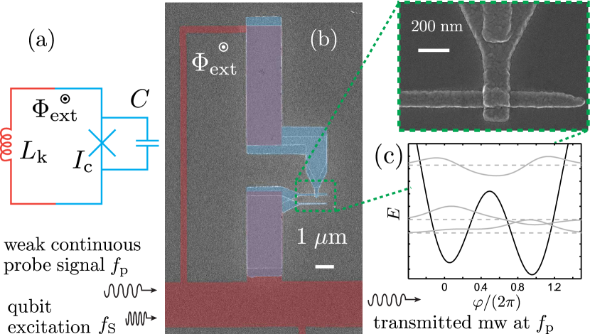
Figure 1 shows a schematic of a hybrid rf SQUID of the above type: The superconducting loop has total kinetic inductance , giving rise to the inductive energy scale . Likewise, the junction has critical current and capacitance , resulting in the Josephson energy and charging energy . The SQUID loop is placed in a perpendicular external magnetic field , giving rise to the flux threading the loop. Figure 1 further shows a sketch of the SQUID double well potential (see, for example, Ref. wendin06, ), as well as the three lowest energy levels and wave functions calculated for , and the representative parameters , , and , yielding . These values corresponding to device I in Fig. 2. Here, the control phase is related to the externally applied biasing magnetic flux via .
II Sample details
Fabrication of the hybrid structure is a technologically challenging problem. The key element is a galvanic contact between the thin film of the highly disordered material and Al. The false color scanning electron micrograph in Fig. 1 illustrates a typical single rf SQUID studied in this work, together with a sketch of the measurement setup. The approximately wide TiN wire that provides the kinetic inductance is shaded in red, whereas the Al-AlOx-Al JJ, fabricated by two-angle shadow evaporation and closing the TiN loop, is highlighted in blue. The two large TiN–Al contact overlap areas are colored purple. The bottom TiN loop edge doubles as part of the wide resonator center line, widening to outside the center section with the SQUID loops. This shared mutual kinetic inductance facilitates the inductive SQUID–resonator coupling.
To pattern inductances from the TiN films, we used a process similar to Refs. peltonen13, and peltonen16, , relying strongly on electron beam lithography (EBL). The starting point is an oxidized Si wafer onto which a thin film of TiN with thickness is grown by atomic layer deposition (ALD) coumou13 ; coumou13b ; bueno15 . This TiN film is identical to film A in Ref. coumou13b, . First, a mask for the CPW resonator ground planes [not visible in Fig. 1 ] as well as coplanar transmission lines for connecting to the microwave measurement circuit is defined by EBL. These structures are consequently metallized in an electron gun evaporator with Ti, Au, and Al on top. After liftoff, another layer of resist is applied by spin coating, and patterned in a second step of EBL to act as an etch mask for the TiN loops and the resonator center line, i.e., the structures highlighted in red in Fig. 1 . The pattern is transferred into the TiN film by reactive ion etching (RIE) with plasma.
Following the etching step, the remaining resist is removed, and a new bilayer resist is applied to prepare for the last EBL step for defining the Josephson junction, blue in Fig. 1 , to close the TiN loop. After development, the mask is loaded into an UHV e-gun evaporator. Crucially, prior to Al deposition the exposed TiN contact surfaces, purple in in Fig. 1 , are cleaned by a brief in-situ Argon ion milling. Immediately after this, the typically thick Al electrodes of the JJ are deposited by conventional shadow evaporation at two different tilt angles. The two Al depositions are separated by an in-situ oxidation in a 10%–90% mixture of and Ar to form the AlOx tunnel barrier. To protect the TiN film from oxidation, the samples were stored under nitrogen atmosphere, and cooled down within 1–2 days after removing the protective resist. The resonator chip was enclosed in a sample box, and microwave characterization was performed in a dilution refrigerator at the base temperature close to . Samples from several fabrication rounds with differing Ar ion cleaning and oxidation parameters were cooled down. Here we present measurement results belonging to one typical sample.
From low temperature dc transport measurements of separate test structures, we infer sufficient quality of the TiN–Al contacts, supporting supercurrents , the critical current of the SQUID Al junction, and showing no significant suppression of the transition temperature of the TiN film due to the Ar ion cleaning. Similarly, suitable JJ oxidation parameters were determined by room temperature resistance measurements of a series of junctions with differing overlap areas.
III Microwave characterization
To characterize the devices we use a vector network analyzer to monitor the transmission of microwaves through the resonator, at probing frequencies close to one of the resonant modes , . Here, denotes the resonator length and the effective speed of light, expressed in terms of (), the inductance (capacitance) per unit length. The samples reported here contain a resonator with , resulting in the fundamental mode frequency with loaded quality factor .
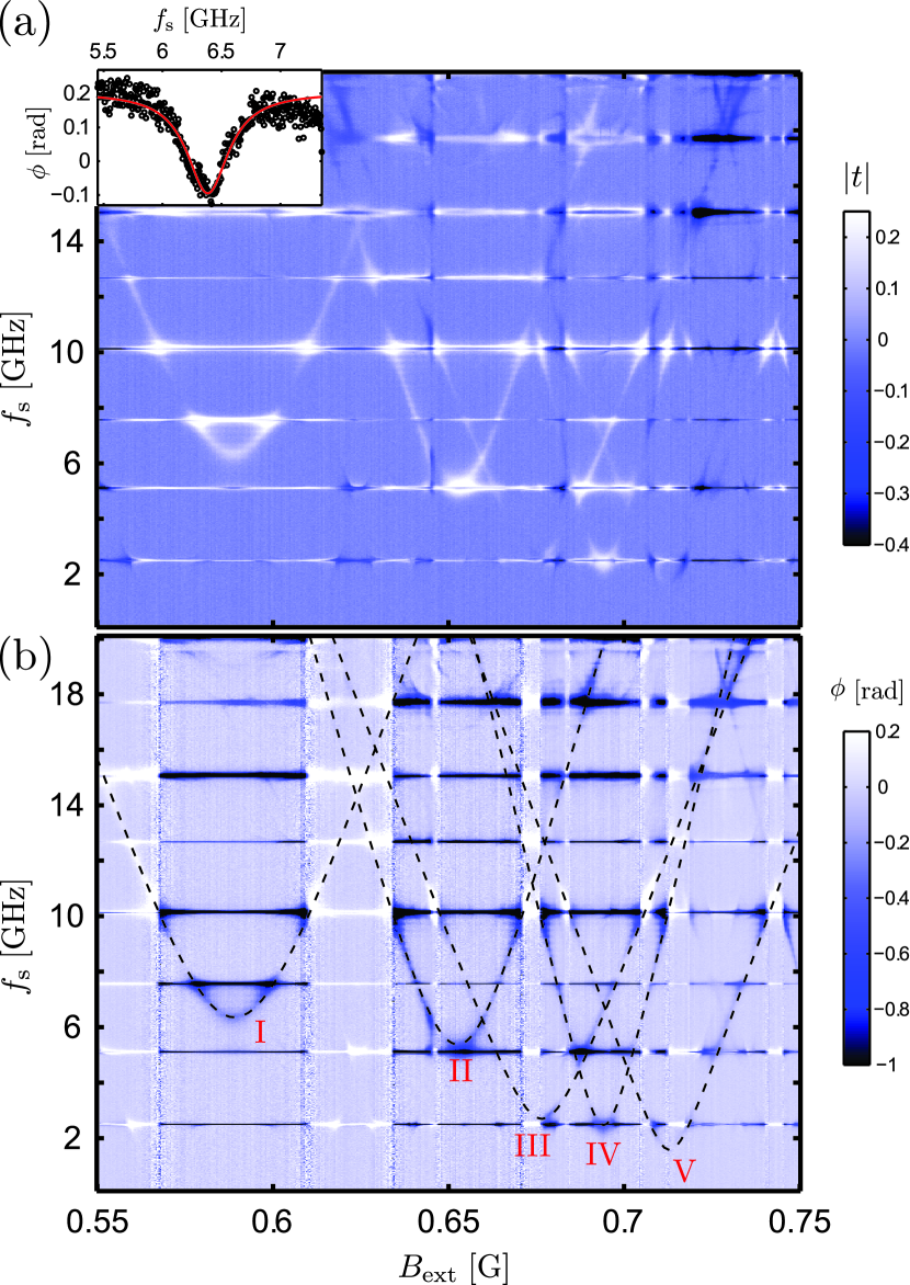
Signatures from the SQUID loops become visible as the global external magnetic field is scanned. In a typical initial test this is done over a period corresponding to of several flux quanta through the loops. At the input port of the resonator, the low-power probing tone at frequency is combined with another continuous microwave signal at frequency for exciting the qubits. A representative result of such two-tone spectroscopy is illustrated in the top panel of Fig. 2, focused on a range of with transitions belonging to five loops coupled to the same resonator. In this measurement, showing the magnitude change of the transmission coefficient, the weak probe tone was fixed at while the frequency of the strong drive signal was scanned across a large span.
The bottom panel of Fig. 2 displays the corresponding phase change of , together with dashed lines indicating qubit transition frequencies calculated according to the standard rf SQUID Hamiltonian wendin06
| (1) |
They are obtained by finding the lowest energy eigenstates by exact diagonalization. In Eq. (1), the number operator of the charge on the junction capacitor and the phase operator obey the commutation relation . Close to , the shape of the curves is well approximated by . Here with denotes the persistent current, and we introduced the flux deviation from degeneracy, .
The inset of Fig. 2 further shows the spectroscopy signal lineshape for the SQUID with (device I the main plot), in the low power limit of the spectroscopy tone, together with a Lorentzian fit. For different devices, we find typical HWHM values between at the optimal point, depending on the detuning from the nearest resonator modes and transitions due to the other SQUID loops. We emphasize that this is the first study of the hybrid TiN–Al devices, and the coherence can be further improved by optimizing the geometry and improving the film quality.
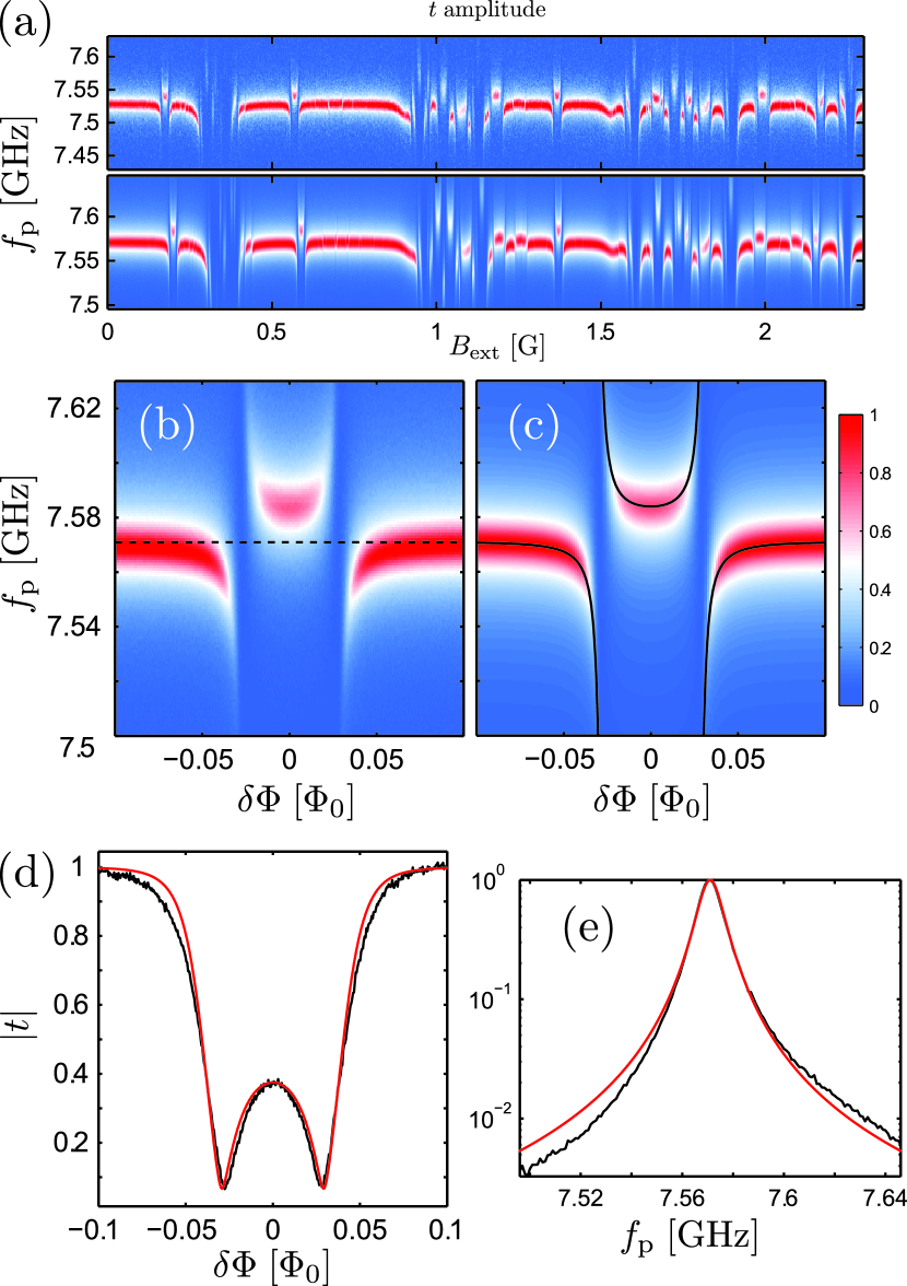
Figure 3 compares the -dependent transmission amplitudes for around a narrow range centered at . The two panels correspond to two nominally identical samples cooled down simultaneously, demonstrating good reliability of the TiN – Al contacts and a promising degree of reproducibility. After detailed analysis of the periodicities of the various features, we detect fingerprints from 23 out of the total 30 SQUID loops, with the largest predicted values of . The remaining devices with are likely to be functional as well, although with too weak coupling for their features to be resolved in this measurement. The bottom panel corresponds to the sample in Fig. 2 as well as Fig. 4 below.
The behavior of at the individual anticrossings due to the qubit transitions can be modeled accurately using a model based on a standard Lindblad master equation oelsner10 ; peltonen13 . In panel of Fig. 3 we show in an enlarged view the measured features in the normalized transmission amplitude due to the anticrossings of a single qubit (device I in Fig. 2). The plot is a zoom-in to a short section of the data in the bottom panel of Fig. 3 . Panel 3 displays the transmission amplitude calculated with the master equation-based model oelsner10 ; peltonen13 , in good agreement with the measurement.
The black solid lines indicate the -dependence of two of the eigenstates of the hybridized qubit–resonator system. The horizontal black dashed line shows the bare resonator frequency , the value of at which the 1D line cuts of in Fig. 3 are plotted as a function of . In panel we further plot the bare resonator transmission for around as the black solid line, at a constant when all the qubit transitions are well detuned from this resonator mode. The red line is a Lorentzian fit included for reference.
After comparisons [as in Fig. 3 –] of the transmission measurements with the theoretical model for several qubit transitions visible in both of the two resonators presented in Fig. 3 , we can indirectly approximate the scatter in to be less than 5 % for the qubits with the largest . For the initial samples reported here all the SQUIDs had different parameters by design, mainly the combination of the loop length and junction size. In addition, the number of of well-isolated features is limited due to the large number of loops in each resonator. To get a more accurate estimate of the fabrication scatter in and other device properties, future experiments will therefore investigate fewer nominally identical SQUIDs coupled to the same resonator, and include a detailed comparison of two nominally identical resonators.
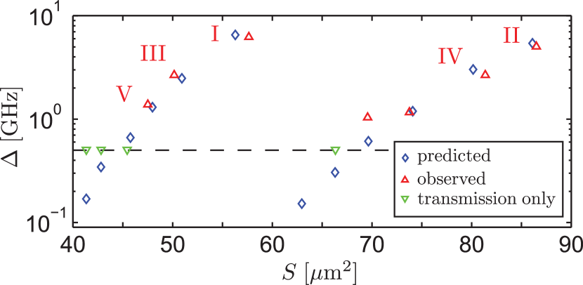
In Fig. 4 we collect together the minimum qubit energy gaps at the optimal flux points, for one of the measured chips. They are shown as the red upward-pointing triangles, extracted from fits to two-tone spectroscopy measurements similar to Fig. 2. Our present scheme is sufficient for resolving qubits in two-tone spectroscopy if . Devices with remain visible in direct transmission measurements, cf. Fig. 3. However, the exact value for in this case can be only indirectly inferred from a comparison of the numerically simulated transmission coefficient with the measurement. For this leads to a large uncertainty, and hence these devices with low are indicated at (green down-triangles).
The experimental values of are plotted against the effective loop area , deduced from the -periodicity of the spectroscopy lines. Analogously, for the SQUIDs with the lowest , the values of were determined by the -periodicity of features in direct transmission measurements.
The sawtooth behavior evident in vs. in Fig. 4 is due to the designed variation in the JJ width. On the other hand, the inductive energy was designed to decrease monotonously with increasing loop area , corresponding further to increasing . To compare these observed energy gaps with theoretical predictions, we use the rf SQUID Hamiltonian of Eq. 1. As input parameters we use the sheet kinetic inductance determined independently from the resonator properties, as well as the nominal loop areas and the number of squares of TiN in each of loops. In addition, we use JJ overlap areas obtained from SEM observations. They differ from the nominal design overlaps, by a approximately constant offsets of and in the width and the height of the junction, respectively. Then, using as adjustable parameters only the values and of the specific junction capacitance and critical current, respectively, we find reasonable agreement between the predictions of the model (blue diamonds) and the experimental observations. Notably, we assume the same values for these oxidation parameters for all the junctions.
IV Conclusions
In summary, we have developed and investigated properties of hybrid rf SQUID qubits relying on the high kinetic inductance of a thin, disordered superconducting film. We find reasonable reproducibility of the device parameters. Future samples will benefit from having only one qubit coupled to a single, hanger-style resonator, several of which can be multiplexed to a single readout transmission line. We note that a somewhat thicker TiN film can be straightforwardly used for forming an equally large loop inductance, in the form of a meander. Then, making the contact is likely to be easier as well as the qubits to be subjected to less dissipation. Moreover, the Ar milling step can be further separately optimized.
Due to the robust fabrication process, the hybrid rf SQUIDs can be employed as a characterization tool and to provide a further control check of decoherence in phase-slip qubits, pointing towards film losses. The present work, demonstrating the ability to create good contact between the thin TiN film and subsequently evaporated Al structures, will be further relevant for dc transport measurements dealing with phase-slip physics of Josephson junctions in highly inductive environments.
Acknowledgements.
We thank K. Kusuyama for assistance with sample fabrication. The work was financially supported by the JSPS FIRST program, and MEXT Kakenhi ’Quantum Cybernetics’. J. T. P. acknowledges support from Academy of Finland (Contract No. 275167). O. V. A. thanks Russian Science Foundation (grants N 15-12-30030 and N 16-12-00070) for support of this work. T. M. K. thanks the support by the Ministry of Education and Science of the Russian Federation, contract No. 14.B25.31.0007 of 26 June 2013, and by the European Research Council Advanced grant no. 339306 (METIQUM).References
- (1) M. H. Devoret and R. J. Schoelkopf, Science 339, 1169 (2013).
- (2) R. Barends, J. Kelly, A. Megrant, A. Veitia, D. Sank, E. Jeffrey, T. C. White, J. Mutus, A. G. Fowler, B. Campbell, Y. Chen, Z. Chen, B. Chiaro, A. Dunsworth, C. Neill, P. O Malley, P. Roushan, A. Vainsencher, J. Wenner, A. N. Korotkov, A. N. Cleland, and J. M. Martinis, Nature 508, 500 (2014).
- (3) A. M. Zagoskin, Superconducting Quantum Metamaterials, In "Nonlinear, Tunable and Active Metamaterials", Ed. I. V. Shadrivov, M. Lapine, and Y. S. Kivshar, (Springer International Publishing, Cham, 2014), pages 255–279.
- (4) P. Macha, G. Oelsner, J.-M. Reiner, M. Marthaler, S. André, G. Schön, U. Huebner, H.-G. Meyer, E. Il’ichev, and A. V. Ustinov, Nat. Commun. 5, 5146 (2014).
- (5) I. Chiorescu, Y. Nakamura, C. J. P. M. Harmans, and, J. E. Mooij, Science 299, 1869 (2003).
- (6) F. Yan, S. Gustavsson, A. Kamal, J. Birenbaum, A. P. Sears, D. Hover, D. Rosenberg, G. Samach, T. J. Gudmundsen, J. L. Yoder, T. P. Orlando, J. Clarke, A. J. Kerman, and W. D. Oliver, Nat. Commun. 7, 12964 (2016).
- (7) J.-L. Orgiazzi, C. Deng, D. Layden, R. Marchildon, F. Kitapli, F. Shen, M. Bal, F. R. Ong, and A. Lupascu, Phys. Rev. B 93, 104518 (2016).
- (8) A. B. Zorin and F. Chiarello, Phys. Rev. B 80, 214535 (2009).
- (9) J. Koch, V. Manucharyan, M. H. Devoret, and L. I. Glazman, Phys. Rev. Lett. 103, 217004 (2009).
- (10) V. E. Manucharyan, J. Koch, L. Glazman, and M. H. Devoret, Science 326, 113 (2009).
- (11) U. Vool, I. M. Pop, K. Sliwa, B. Abdo, C. Wang, T. Brecht, Y. Y. Gao, S. Shankar, M. Hatridge, G. Catelani, M. Mirrahimi, L. Frunzio, R. J. Schoelkopf, L. I. Glazman, and M. H. Devoret, Phys. Rev. Lett. 113, 247001 (2014).
- (12) I. M. Pop, K. Geerlings, G. Catelani, R. J. Schoelkopf, L. I. Glazman, and M. H. Devoret, Nature 508, 369 (2014).
- (13) G. Rastelli, M. Vanevic, and W. Belzig, New J. Phys. 17, 053026 (2015).
- (14) G. Viola and G. Catelani, Phys. Rev. B 92, 224511 (2015).
- (15) N. A. Masluk, I. M. Pop, A. Kamal, Z. K. Minev, and M. H. Devoret, Phys. Rev. Lett. 109, 137002 (2012).
- (16) M. T. Bell, I. A. Sadovskyy, L. B. Ioffe, A. Yu. Kitaev, and M. E. Gershenson, Phys. Rev. Lett. 109, 137003 (2012).
- (17) G. Wendin and V. S. Shumeiko, Superconducting Quantum Circuits, Qubits and Computing, In "Handbook of Theoretical and Computational Nanotechnology", Ed. M. Rieth and W. Schommers, (American Scientific Publishers, Los Angeles, 2006), Volume 3, pages 223–309.
- (18) J. R. Friedman, V. Patel, W. Chen, S. K. Tolpygo, and J. E. Lukens, Nature 406, 43 (2000).
- (19) K. K. Likharev, Dynamics of Josephson Junctions and Circuits, (Gordon and Breach, New York, 1986).
- (20) J. E. Mooij and C. J. P. M. Harmans, New J. Phys. 7, 219 (2005).
- (21) J. E. Mooij and Yu. V. Nazarov, Nat. Phys. 2, 169 (2006).
- (22) O. V. Astafiev, L. B. Ioffe, S. Kafanov, Yu. A. Pashkin, K. Yu. Arutyunov, D. Shahar, O. Cohen, and J. S. Tsai, Nature 484, 355 (2012).
- (23) J. T. Peltonen, O. V. Astafiev, Yu. P. Korneeva, B. M. Voronov, A. A. Korneev, I. M. Charaev, A. V. Semenov, G. N. Gol’tsman, L. B. Ioffe, T. M. Klapwijk, and J. S. Tsai, Phys. Rev. B 88, 220506(R) (2013).
- (24) W. Guichard and F. W. J. Hekking, Phys. Rev. B 81, 064508 (2010).
- (25) A. Di Marco, F. W. J. Hekking, and G. Rastelli, Phys. Rev. B 91, 184512 (2015).
- (26) T. Weissl, G. Rastelli, I. Matei, I. M. Pop, O. Buisson, F. W. J. Hekking, and W. Guichard, Phys. Rev. B 91, 014507 (2015).
- (27) V. E. Manucharyan, N. A. Masluk, A. Kamal, J. Koch, L. I. Glazman, and M. H. Devoret, Phys. Rev. B 85, 024521 (2012).
- (28) J. T. Peltonen, Z. H. Peng, Yu. P. Korneeva, B. M. Voronov, A. A. Korneev, A. V. Semenov, G. N. Gol’tsman, J. S. Tsai, and O. V. Astafiev, Phys. Rev. B 94, 180508(R) (2016).
- (29) P. C. J. J. Coumou, M. R. Zuiddam, E. F. C. Driessen, P. J. de Visser, J. J. A. Baselmans, and T. M. Klapwijk, IEEE Trans. Appl. Super. 23, 7500404 (2013).
- (30) P. C. J. J. Coumou, E. F. C. Driessen, J. Bueno, C. Chapelier, and T. M. Klapwijk, Phys. Rev. B 88, 180505(R) (2013).
- (31) J. Bueno, P. C. J. J. Coumou, G. Zheng, P. J. de Visser, T. M. Klapwijk, E. F. C. Driessen, S. Doyle, and J. J. A. Baselmans, Appl. Phys. Lett. 105, 192601 (2014).
- (32) G. Oelsner, S. H. W. van der Ploeg, P. Macha, U. Hübner, D. Born, S. Anders, E. Il’ichev, H.-G. Meyer, M. Grajcar, S. Wünsch, M. Siegel, A. N. Omelyanchouk, and O. V. Astafiev, Phys. Rev. B 81, 172505 (2010).