Characterization of individual layers in a bilayer electron system produced in a wide quantum well
Abstract
Here we report on a transparent method to characterize individual layers in a double-layer electron system which forms in a wide quantum well and to determine their electron densities. The technique relies on the simultaneous measurement of the capacitances between the electron system and gates located on either side of the well. Modifications to the electron wave function due to the population of the second subband and appearance of an additional electron layer can be detected. The magnetic field dependence of these capacitances is dominated by quantum corrections caused by the occupation of Landau levels in the nearest electron layer. The technique should be equally applicable to other implementations of a double layer electron system.
I INTRODUCTION
Double-layer electron systems (DLESs) composed of a pair of coupled two-dimensional electron systems (2DESs) have attracted considerable attention due to the rich variety of collective phenomena they host Ref1 . Of particular interest has been the equilibrium superfluid exciton condensate which emerges when the total number of electrons in the double layer system equals the degeneracy of a single spin split Landau level (see review article Eisen2 and Refs. therein). While nearly all previous experiments were performed on GaAs/AlGaAs heterostructures, this activity has recently received renewed impulse from both theoretical MacDon ; Perali and experimental Tutuc ; Kim studies on graphene-based devices.
In GaAs/AlGaAs heterostructures the double layer system is formed either in a double quantum well device Boebinger or in a wide quantum well (QW) exhibiting a confinement potential with two minima located near the left and right barrier Suen . In the wide quantum well implementation, the electron layers can not be contacted separately, since annealed ohmic contacts short-circuit the two layers. In double quantum well structures suitable methods and sample designs have been developed EisenMes (see also recent paper Ritchie and Refs. therein) to separately contact the individual layers. This has enabled a far wider variety of experiments including interlayer tunneling and electron drag studies which have led to the discovery of a Bose-Einstein exciton condensate in this double layer system.
Because the fabrication of separately contacted double layer systems remains challenging, many studies continue to be carried out using simultaneously contacted 2DESs. In such cases, an essential task is the determination of the electron densities in the individual layers or subbands. This is usually attempted by analyzing the Shubnikov-de Haas oscillations (SdHO), which are periodic in the inverse of the magnetic field, using Fourier transform techniques. In a single 2DES the minima of SdHO correspond to filling of integer numbers of spin split Landau levels and their magnetic field positions satisfy the condition , where is the electron areal density, represents the degeneracy of a single spin split Landau level, and or 2 depending on whether spin splitting is resolved or not. The SdHO frequency in the inverse magnetic field is equal to . Therefore, in a single 2DES the fundamental frequency () is observed at low magnetic fields when spin splitting is not resolved, whereas at higher field strength the harmonic with may appear. In DLESs the number of Fourier harmonics increases and the frequencies determined by the electron densities of the individual layers are complemented by their sum and difference. Namely, the frequency (here and are electron densities in two individual layers) originates from magnetointersubband oscillations Polyan ; Coleridge ; PRB46 ; Gusev ; Raikh brought about by elastic intersubband scattering of electrons. The frequency has been associated with so-called single-layer behavior Ritchie1996 involving the redistribution of electrons among the layers Ritchie1996 ; Dorozh2016 . The relative strength of different frequencies strongly depends on temperature PRB46 ; Gusev since the magnetointersubband oscillations in contrast to SdHO are not sensitive to the temperature broadening of the Fermi distribution function Polyan ; Raikh . For a more detailed discussion of the Fourier analysis of magnetoresistance oscillations we refer the reader to the supplementary material Supp in Ref. Ensslin .
II SAMPLES AND EXPERIMENTAL TECHNIQUE
Capacitance measurements have been widely used for the characterization of the distribution of electric charges in semiconductors. In field-effect transistors containing a 2DES they also allow studying the compressibility of the electronic system Stiles ; Krav1 ; EisenPRL ; Krav2 ; DorozhPRB2 as well as the energy gaps of incompressible integer Stiles ; KhrpaiPRLI and fractional quantum Hall ground states that may form DorozhCap1993 ; Eisen1994 ; DorozhPRB1995 ; KhrpaiPRL . The capacitance technique was also previously used in experiments on DLESs EisenPRL ; Ensslin2 ; Dolgopolov1 ; Dolgopolov2 , however the compressibility of only one of the layers was measured. Here we extend the capacitance method to get access to the compressibility of the two individual layers in a wide quantum well. We show that it is possible to detect the integer filling of the Landau levels in each layer and, hence, to determine their individual electron densities.
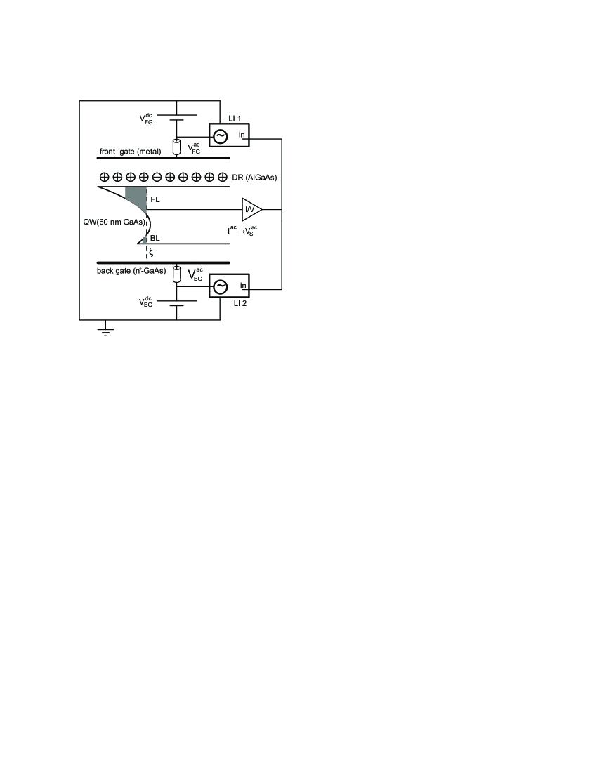
This study has been performed on a Hall bar sample processed from a GaAs/AlGaAs heterostructure (see the experimental layout in Fig.1) where the electron system resides in a 60 nm wide GaAs quantum well (QW) located 140 nm below the sample surface. A homogeneously doped in-situ grown GaAs layer 850 nm below the QW served as a back gate. The QW was filled with electrons via modulation doping of the top AlGaAs layer at a distance of 65 nm from the QW. A Schottky front gate was created by evaporating a thin gold film on the sample surface. By changing the dc voltages between the electron system and the gates (front gate, , and back gate, ) the total electron density was varied in the range . Increasing resulted in the population of the second subband of the wide QW and gave rise to the formation of the second layer closer to the back gate as schematically illustrated in Fig.1. This will be confirmed experimentally below. The ohmic contacts to the electronic system shaped into a Hall bar enabled the acquisition of both the longitudinal and Hall resistances (For the sake of simplicity, only one contact is shown in Fig.1). The measurements were carried out with the sample immersed in liquid in the presence of a tunable magnetic field perpendicular to the QW-plane.
III RESULTS AND DISCUSSION
The capacitances between the electronic system and both gates were measured simultaneously using two dual-phase lock-in amplifiers (LI1 and LI2). To measure capacitances, the gate voltages were modulated with ac voltages and with different frequencies between 10 and 300 Hz produced by the internal oscillators of the lock-in amplifiers. The induced ac currents were added and converted to an ac voltage, , with a transimpedance amplifier. The two frequency components were detected separately with the two lock-in amplifiers. The out-of-phase and in-phase signals from both amplifiers were measured simultaneously. To minimize the stray capacitance, the gates were connected to coaxial cables. However, some stray capacitance remained in particular for the back gate which couples not only to the electronic system but also to the ohmic contact areas. This stray capacitance has been directly measured under conditions where the integer quantum Hall effect is well-developed. In this regime, the dissipative conductivity of the 2DES tends to zero and the bulk of the electronic system is not charged at the modulation frequencies used in the experiment DorozhJETPL1986 . For a highly conducting 2DES, the out-of-phase signal is proportional to the capacitance. It includes the quantum correction brought about by the finite compressibility of the 2DES Stiles (for zero magnetic field see also Ref. Luryi ). For a field-effect transistor composed of a 2DES in a narrow quantum well and a single gate the equation for the capacitance reads as Stiles ,
| (1) |
where is the gated area of the sample, the chemical potential of the 2DES and the geometric capacitance with the thickness of the insulating layer with dielectric permittivity separating the gate and the center of weight of the electron wave function in the quantum well. The second term is inversely proportional to the electronic compressibility . This term gives rise to capacitance minima when the electronic system turns less compressible at magnetic fields where the chemical potential is located in between Landau levels, i.e. near integer fillings of the Landau levels.
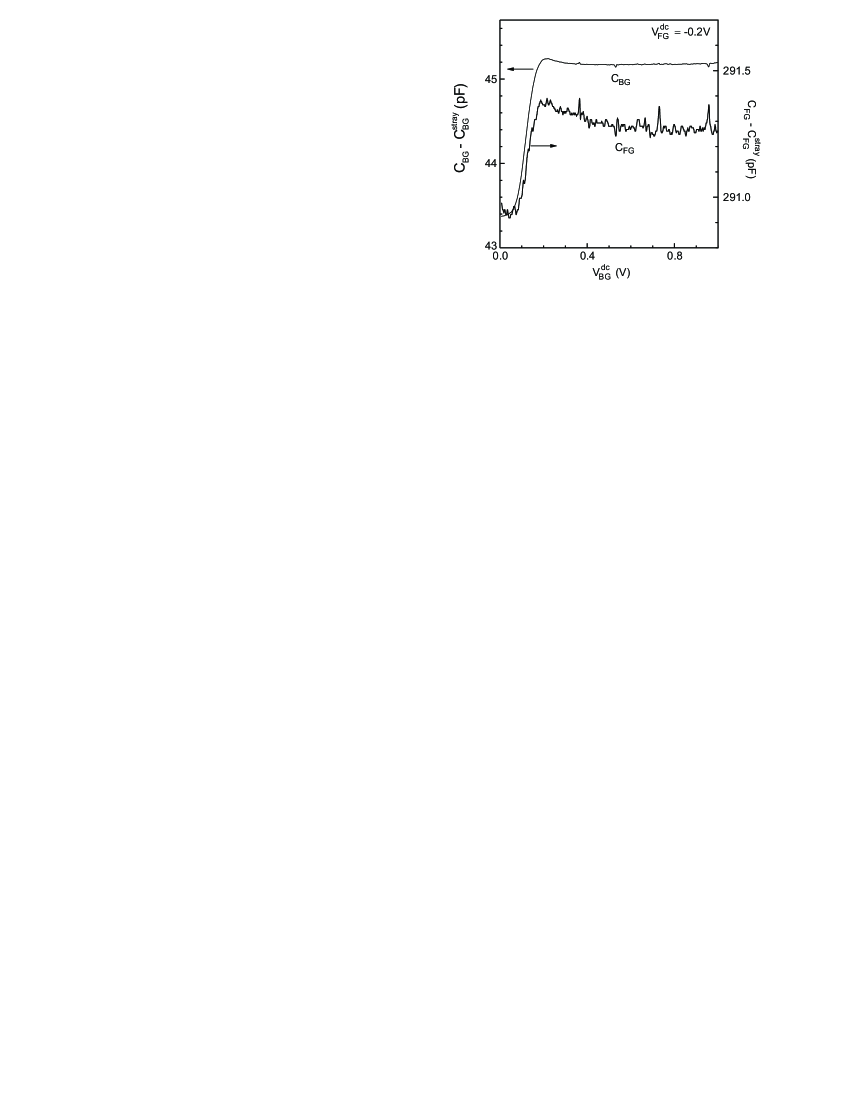
The formation of a second layer or occupation of the second subband is demonstrated in Fig. 2. Shown are variations of the front and back gate capacitances with back gate voltage. Near V both capacitances display an abrupt increase. The back (front) gate capacitance rises by about 1.8 pF (0.4 pF) or 4% (0.14%). In terms of a classical planar capacitor this would correspond to a decrease of the distance between the capacitor plates of approximately 34 nm (0.2 nm) for the given distance of 850 nm (140 nm) between the QW and the back (front) gate. These results imply that electrons start to occupy the second subband and a new layer (back layer, BL) is formed, located about 34 nm closer to the back gate than the ground subband layer, i.e. front layer (FL) Comment1 . At , the center of weight of the wave function in the ground subband is hardly affected by the occupation of the second subband. It practically does not change also when raising V, i.e. with increasing electron density in the second subband.
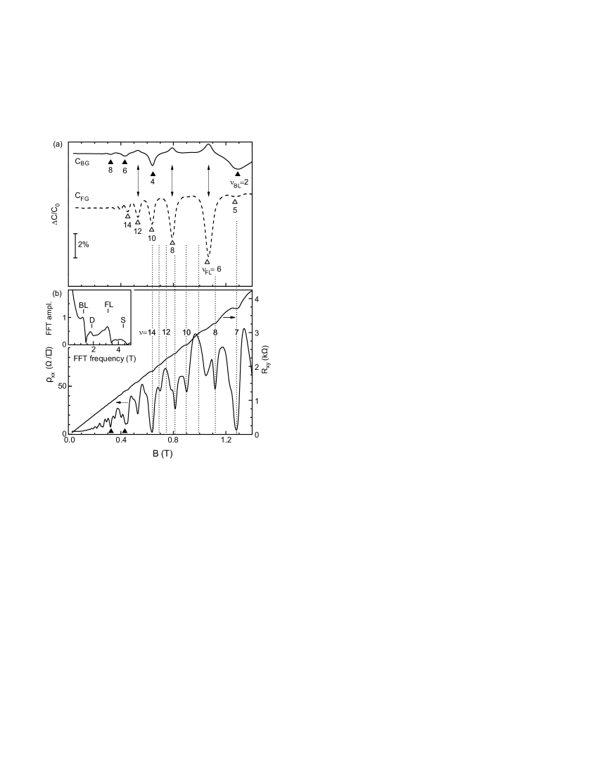
Typical magnetocapacitance data are presented in Fig. 3(a). Each curve shows one set of minima whose positions are periodic in the inverse magnetic field. The periods are distinct for the and curves. Based on the previous magnetocapacitance studies of 2DES, we ascribe these magnetocapacitance minima to the integer filling of the Landau levels in the layer adjacent to a particular gate. From these oscillations, we determine the areal electron densities in both layers and mark the positions of the corresponding integer filling factors using numbered triangles (see Fig.3(a)).
It is instructive to compare the magnetocapacitance data with the magnetoresistance oscillations shown in Fig.3(b). Note the complicated behavior of these oscillations at T. Some of the magnetoresistance minima can be assigned to integer filling () of a 2DES with an electron density . The same density is extracted from the Hall resistance. However, there are no minima at and hence the sequence of oscillations is not periodic in the inverse of the magnetic field. For T the magnetoresistance minima in general do not coincide with any of the magnetocapacitance features. However, when the filling factor of both layers takes on an integer value (, and , ), the magnetoresistance shows deep minima ( and 14), which are accompanied by quantum Hall plateaus. For T the oscillation pattern exhibits two different frequencies. Two of the low frequency minima nearly coincide with and as indicated by the solid triangles in panel (b).
It is also informative to compare the electron densities obtained from the magnetocapacitance data with those determined from the Fourier spectrum analysis of the magnetoresistance oscillations displayed in the inset to Fig. 3(b). Four maxima can be identified in the spectrum. Two of them correspond to the oscillations from the individual layers as they are located rather close to the frequencies determined from the magnetocapacitance data (marked as BL and FL). Two other maxima lie at the sum (S) and difference (D) of these frequencies. Hence, in general, the determination of the electron densities from a Fourier spectrum requires careful analysis. Our comparison of the two methods illustrates that the magnetocapacitance data enable a straightforward interpretation and ensure a markedly improved accuracy.
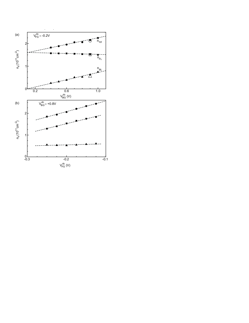
The electron densities determined from the magnetocapacitance data are shown in Fig.4 for different front- and back-gate voltages. The electron density in a layer increases linearly with the voltage applied to the nearest gate and is only slightly affected by the voltage on the gate separated by the other layer. In the latter case the electron density dependence may even possess a negative slope (see the dependence in Fig.4(a)). This is common in bilayer systems and has been attributed Millard ; Smet to exchange correlation induced negative compressibility EisenPRL of 2D electron systems at low density.
At first sight, the capacitance data look like those for two independent 2DES. However, the effect of coupling between the layers can be seen in Fig.3(a) as maxima on the curve at the positions of some () minima of the dependence. These features are highlighted by double-sided arrows.
IV CONCLUSION
In summary, we have shown that, compared to the magnetoresistance measurements, our capacitance technique reveals effects of Landau quantization in individual layers of a double-layer electron system produced in a wide quantum well. In particular, this method enables accurate determination of electron densities in each layer despite the absence of separate contacts to each layer.
Acknowledgements.
The experiment and data evaluation of this work were supported by the Russian Foundation for Basic Research (Grant 17-02-00769). JHS and VU acknowledge support from the GIF.References
- (1) see experimental chapter by J. P. Eisenstein and theoretical chapter by S. M. Girvin and A. H. MacDonald, in Das Sarma S. and Pinczuk A. (ed) 1997 Perspectives on Quantum Hall Effects (New York: Wiley)
- (2) J. P. Eisenstein, Annu. Rev. Condens. Matter Phys. 5, 159 (2014). Exciton Condensation in Bilayer Quantum Hall Systems.
- (3) H. Min, R. Bistritzer, J-J. Su, and A. H. MacDonald, Phys. Rev. B 78, 121401 (2008). Room-temperature superfluidity in graphene bilayers.
- (4) A. Perali, D. Neilson, and A. R. Hamilton, Phys. Rev. Lett. 110, 146803 (2013). High-Temperature Superfluidity in Double-Bilayer Graphene.
- (5) K. Lee, B. Fallahazad,J. Xue, D.C. Dillen, K. Kim, T. Taniguchi, K. Watanabe, E. Tutuc, Science 345, 58 (2014). Chemical potential and quantum Hall ferromagnetism in bilayer graphene.
- (6) X. Liu, K. Watanabe, T. Taniguchi, B. I. Halperin, and P. Kim, Nat. Phys. 13, 746 (2017). Quantum Hall drag of exciton condensate in graphene.
- (7) G. S. Boebinger, H. W. Jiang, L. N. Pfeiffer, and K. W. West, Phys. Rev. Lett. 64, 1793 (1990).
- (8) Y. W. Suen, J. Jo, M. B. Santos, L. W. Engel, S. W. Hwang, and M. Shayegan, Phys. Rev. B 44, 5947 (1991).
- (9) J. P. Eisenstein, L. N. Pfeiffer, and K. W. West, Appl. Phys. Lett. 57, 2324 (1990). Independently contacted two-dimensional electron systems in double quantum wells.
- (10) U. S. de Cumis, J. Waldie, A. F. Croxall, D. Taneja, J. Llandro, I. Farrer, H. E. Beere, and D. A. Ritchie, Appl. Phys. Lett. 110, 072105 (2017). A complete laboratory for transport studies of electron-hole interactions in GaAs/ AlGaAs ambipolar bilayers.
- (11) D. R. Leadley, R. Fletcher, R. J. Nicholas, F. Tao, C. T. Foxon, and J. J. Harris, Phys. Rev. B 46, 12439 (1992). Intersubband resonant scattering in heterojunctions.
- (12) N. C. Mamani, G. M. Gusev, T. E. Lamas, and A. K. Bakarov, Phys. Rev. B 77, 205327 (2008). Resonance oscillations of magnetoresistance in double quantum wells.
- (13) V. M. Polyanovskii, Fiz. Tekh. Poluprovodn. 22, 2230 (1988) [Sov. Phys. Semicond. 22, 1408 (1988)].
- (14) P. T. Coleridge, Semicond. Sci. Technol. 5, 961 (1990). Inter-subband scattering in a 2D electron gas.
- (15) M. E. Raikh and T. V. Shahbazyan, Phys. Rev. B 49, 5531 (1994). Magnetointersubband oscillations of conductivity in a two-dimensional electronic system.
- (16) A. G. Davies, C. H. W. Barnes, K. R. Zolleis, J. T. Nicholls, M. Y. Simmons, and D. A. Ritchie, Phys. Rev. B 54, R 17331 (1996). Hybridization of single- and double-layer behavior in a double-quantum-well structure.
- (17) S. I. Dorozhkin, JETP Letters 103, 513 (2016) [Pis’ma v ZhETF 103, 578 (2016)]. Quantum Hall Effect in a System with an Electron Reservoir.
- (18) Supplementary Material at http://link.aps.org/ supplemental/10.1103/PhysRevB.89.081306.
- (19) F. Nichele, A. N. Pal, R. Winkler, C. Gerl, W. Wegscheider, T. Ihn, and K. Ensslin, Phys. Rev. B 89, 081306(R) (2014). Spin-orbit splitting and effective masses in p-type GaAs two-dimensional hole gases.
- (20) T. P. Smith, B. B. Goldberg, P. J. Stiles, and M. Heiblum, Phys. Rev. B 32, 2696(R) (1985). Direct measurement of the density of states of a two-dimensional electron gas.
- (21) S.V. Kravchenko, V.M. Pudalov, S.G. Semenchinsky, Phys. Lett. A 141, 71 (1989). Negative density of states of 2D electrons in a strong magnetic field.
- (22) J. P. Eisenstein, L. N. Pfeiffer, and K. W. West, Phys. Rev. Lett. 68, 674 (1992). Negative Compressibility of Interacting Two-Dimensional Electron and Quasiparticle Gases.
- (23) S. V. Kravchenko, M. Caulfield, J. Singleton, H. Nielsen, and V. M. Pudalov, Phys. Rev. B 47, 12961 (1993). Electron-electron interactions in the two-dimensional electron gas in silicon.
- (24) S.I. Dorozhkin, J.H. Smet, K. von Klitzing, V. Umansky, R.J. Haug, and K. Ploog. Phys. Rev. B 63, 121301 (2001). Comparison between the compressibilities of the zero field and composite-fermion metallic states of the two-dimensional electron system.
- (25) S. I. Dorozhkin, G. V. Kravchenko, R. J. Haug, K. von Klitzing, and K. Ploog, JETP Lett. 58, 834 (1993) [Pis’ma Zh. Eksp. Teor. Fiz. 58, 893 (1993)]. Capacitance spectroscopy of the fractional quantum Hall effect: Temperature dependence of the energy gap.
- (26) J. P. Eisenstein, L. N. Pfeiffer, and K. W. West, Phys. Rev. B 50, 1760 (1994). Compressibility of the two-dimensional electron gas: Measurements of the zero-field exchange energy and fractional quantum Hall gap.
- (27) S. I. Dorozhkin, R. J. Haug, K. von Klitzing, and K. Ploog, Phys. Rev. B 51, 14729 (1995). Experimental determination of the quasiparticle charge and the energy gap in the fractional quantum Hall effect.
- (28) V. S. Khrapai, A. A. Shashkin, M. G. Trokina, V. T. Dolgopolov, V. Pellegrini, F. Beltram, G. Biasiol and L. Sorba, Phys. Rev. Lett. 99, 086802 (2007). Direct Measurements of Fractional Quantum Hall Effect Gaps.
- (29) V. S. Khrapai, A. A. Shashkin, and V. T. Dolgopolov, Phys. Rev. Lett. 91, 126404 (2003). Direct Measurements of the Spin and the Cyclotron Gaps in a 2D Electron System in Silicon.
- (30) K. Ensslin, D. Heitmann, R. R. Gerhardts, and K. Ploog, Phys. Rev. B 39, 12993 (1989). Population process of the upper subband in quantum wells.
- (31) V. T. Dolgopolov, G. E. Tsydynzhapov, A. A. Shashkin, E. V. Deviatov, F. Hastreiter, M. Hartung, A. Wixforth, K. L. Campman, and A. C. Gossard, Pis ma Zh. Eksp. Teor. Fiz. 67, 563 (1998) [JETP Lett. 67, 595 (1998)]. Magnetic-field-induced hybridization of electron subbands in a coupled double quantum well.
- (32) V. T. Dolgopolov, A. A. Shashkin, E. V. Deviatov, F. Hastreiter, M. Hartung, A. Wixforth, K. L. Campman, and A. C. Gossard, Phys. Rev. B 59, 13235 (1999). Electron subbands in a double quantum well in a quantizing magnetic field.
- (33) S. I. Dorozhkin, A. A. Shashkin, N. B. Zhitenev, and V. T. Dolgopolov, JETP Lett. 44, 241 (1986) [Pis’ma Zh. Eksp. Teor. Fiz. 44, 189 (1986)]. ”Skin effect” and observation of nonuniform states of a 2D electron gas in a metal-insulator-semiconductor structure.
- (34) S. Luryi, Appl. Phys. Lett. 52, 501 (1988). Quantum capacitance devices.
- (35) We note that this estimate assumes infinite electron compressibility in the layers, which affects its accuracy.
- (36) I. S. Millard, N. K. Patel, M. Y. Simmons, E. H. Linfield, D. A. Ritchie, G. A. C. Jones, and M. Pepper, Appl. Phys. Lett. 68, 3323 (1996). Compressibility studies of double electron and double hole gas systems.
- (37) D. Zhang, S. Schmult, V. Venkatachalam, W. Dietsche, A. Yacoby, K. von Klitzing, and J. Smet, Phys. Rev. B 87, 205304 (2013). Local compressibility measurement of the quantum Hall state in a bilayer electron system.