Granular-composite-like electrical transport properties of polycrystalline cubic TaNx thin films prepared by rf sputtering method
Abstract
We have systematically investigated the electrical transport properties of polycrystalline TaNx (1.32) films with rocksalt structure from 300 down to 2 K. It is found that the conductivity varies linearly with from 6 K to 30 K, which does not originate from the conventional two dimensional weak-localization or electron-electron interaction effects, but can be well explained by the intergrain Coulomb effect which was theoretically proposed in the granular metals. While the fluctuation-induced tunneling conduction process dominates the temperature behaviors of the conductivities (resistivities) above 60 K. Normal state to superconductive state transition is observed in the 1.04 films in low temperature regime. The superconductivity can still be retained at a field of 9 T. The upper critical field increases linearly with decreasing temperature in the vicinity of the superconductive transition temperature, which is the typical feature of granular superconductors or dirty type-II superconductors. The granular-composite-like electrical transport properties of the polycrystalline TaNx films are related to their microstructure, in which the TaNx grains with high conductivity are separated by the poorly conductive amorphous transition layers (grain boundaries).
I Introduction
During the last decades, tantalum nitride (TaNx) with rocksalt structure has received much attention due to its high hardness no1 , good wear resistance no2 , chemical inertness no3 , thermodynamic stability no4 , and low temperature coefficients of resistivity no5 . Besides these excellent properties, the TaNx in rocksalt structure possesses superconductivity at liquid helium temperatures and has a small superconducting energy gap, thus it is potential candidate material for superconducting nanowire single-photon detectors no6 . In addition, the resisitivity of the rocksalt TaNx can be as low as cm, which makes TaNx be good examplary material for investigating the abundant physics near superconductor-insulator transition no7 ; no8 ; sup . Although the TaNx films have been technologically applied in many fields, some fundamental issues are still not clear. For example, the density-functional theory (DFT) calculation results indicate that TaNx in the rocksalt structure has a metallic nature in energy-band structure no9 ; no10 . However, numerous experimental results show TaNx in the rocksalt structure has negative temperature coefficient of resistivity (TCR, here TCR is defined as , and is the resistivity at a certain temperature ) no5 ; no11 , and the origins of the negative TCR is still debatable. Tiwari et al ascribed the negative TCR of TaN films to weak-localization effect no12 , while the hopping conduction and electron-electron (e-e) interaction effect were considered as the origins by other groups no13 ; no14 . Thus further investigations on the fundamental properties, especially with regard to the electrical transport properties, are still needed for the TaNx compounds. In the present paper, we investigate the electrical transport properties of rocksalt TaNx thin films with . The cross-section high resolution electron transmission microscopy images and transport results indicate the TaNx thin films are similar to the ‘conductor-insulator granular composites’ in morphologies and electrical transport properties, respectively. In additions, it is found that a field of up to 9 T cannot destroy the superconductivity of the TaNx films with . We report our results in the following discussions.
II Experimental Method
The samples were deposited on quartz glass substrates by rf sputtering method. The size of the substrate is mm10 mm. Considering Ta-N compounds can exhibit a variety of crystallographic phases such as cubic, hexagonal, and tetragonal, we chose a commercial TaN target, in which the nominal atomic ratio of Ta to N is (provided by Shanghai Institute of Optics and Fine Mechanics, Chinese Academic of Science), as the sputtering source to avoid producing impure phases. Indeed, it is found that the rocksalt structure single phase TaNx film can be readily obtained only in Ar atmosphere. The chamber was pre-pumped down to Pa and the argon (99.999% in purity) pressure was maintained at 0.6 Pa during sputtering. The substrate temperature was set as 873 K and the composition of the films was tuned by changing the sputtering power from 70 W to 130 W. We also deposited an amorphous film at room temperature for comparison (sputtering power 130 W). The thicknesses of the films, 150 nm, were measured with a surface profiler (Dektak, 6 M). The crystal structures of the films were measured using a x-ray diffractometer (XRD, D/MAX-2500v/pc, Rigaku) with Cu Kα radiation. The composition of the films was obtained from the energy-dispersive x-ray spectroscopy analysis (EDS). The microstructure of the films was characterized by transmission electron microscopy (TEM, Tecnai G2 F20). The resistivities and Hall effect measurements were carried out in a physical property measurement system (PPMS-6000, Quantum Design) by employing the standard four-probe methods. Hall-Bar-shaped films (1 mm wide, 10 mm long, and the distance between the two voltage electrodes is 3.6 mm) defined by mechanical masks were used for the measurements. For the amorphous film with high resistance, a Keithley 6221 current source and a Keithley 2182A nanovoltmeter were used in the four-probe configuration.
III Results and Discussions
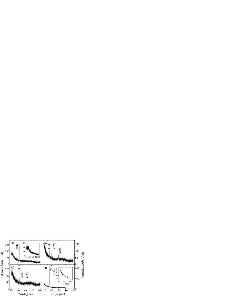
Figure 1 shows the XRD patterns of films deposited at 873 K but different sputtering powers. The inset of Fig. 1 (a) is the diffraction pattern for film deposited at room temperature. There is no sharp peak appear in the pattern, indicating the film is amorphous. When the substrate temperature is enhanced to 873 K, relatively weak diffraction peaks appear. For each film, the diffraction peaks can be indexed based on the face centered cubic structure (rocksalt structure) TaN (PDF No.49-1283), and other phases, such as, hexagonal or tetragonal structure Ta-N compounds are not detected. For the film deposited at 70 W, the preferred growth orientation is along [200] direction. Along with increasing sputtering power, the relative intensity of (111) peak gradually increases while the relative intensity of (200) decreases. When the sputtering power is enhanced to 100 W, the intensity of (111) peak is far greater than that of the diffractions of other planes, i.e., the (111) direction becomes the preferred growth orientation. The inset of Fig. 1 (d) shows the ratio of N to Ta, , varies as a function of sputtering power. The value decreases monotonously with increasing sputtering power. The maximum and minimum values of are 1.32 and 0.83, respectively. Our results indicate that TaNx films could maintain the rocksalt structure in the regime , which is consistent with the results of other groups no1 ; no11 ; no15 . Considering the composition is one of the key elements determining the intrinsic properties of materials, we use TaNx instead of sputtering power to identify our films in the following discussions.
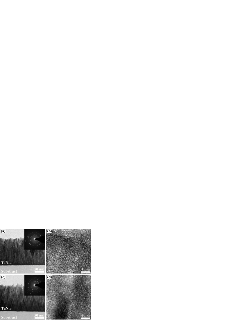
Figure 2 shows the cross-sectional TEM images and selected-area diffraction patterns (insets) of TaN1.32 and TaN1.01 films. From Fig. 2 (a) and (c), one can see that the compact films reveal columnar growth features. From the cross-section images, we can obtain the average thickness of the films, which is identical to that measured in the surface profiler. Figure 2 (b) and (d) present the high resolution TEM images of the films. Inspection of the high resolution TEM images indicates that the mean grain sizes are 5 nm and the TaNx grains are separated by amorphous boundaries with thickness 2 to 3 nm for both films. We note in passing that the selected area electron diffraction (SAED) patterns (insets in Fig. 2) also reveal a pure rocksalt structure of the films.

| (300 K) | (200 K) | ||||||||||
|---|---|---|---|---|---|---|---|---|---|---|---|
| (nm) | (m cm) | ( cm-3) | (S/m) | (m cm) | (K) | (K) | ( K) | (nm) | |||
| 1.32 | 150 | 6.23 | 0.59 | 7762 | 0.80 | 1.33 | 1292 | 536 | 0.414 | 3.11 | 2.20 |
| 1.18 | 155 | 5.42 | 0.75 | 8673 | 0.85 | 1.20 | 1208 | 502 | 0.415 | 2.91 | 2.23 |
| 1.07 | 153 | 5.26 | 1.49 | 10425 | 1.09 | 1.18 | 1364 | 616 | 0.452 | 3.02 | 2.38 |
| 1.04 | 155 | 4.67 | 3.66 | 12981 | 1.67 | 1.14 | 1365 | 667 | 0.489 | 2.79 | 2.87 |
| 1.01 | 145 | 4.24 | 5.44 | 15118 | 1.69 | 0.99 | 1575 | 785 | 0.499 | 3.16 | - |
| 0.97 | 150 | 3.80 | 5.71 | 17742 | 1.86 | 0.91 | 1676 | 872 | 0.520 | 3.22 | - |
| 0.92 | 150 | 3.61 | 11.11 | 19343 | 2.04 | 0.89 | 1704 | 925 | 0.543 | 3.14 | - |
| 0.90 | 152 | 3.15 | 18.60 | 22536 | 2.36 | 0.81 | 1671 | 934 | 0.559 | 2.99 | - |
| 0.83 | 160 | 2.64 | 21.46 | 30228 | 3.70 | 0.74 | 1988 | 1259 | 0.633 | 3.14 | - |
Figure 3 (a) shows the temperature dependence of resistivity for the polycrystalline TaNx films with different , as indicated. The resistivity increases monotonically with decreasing temperature from 300 down to 5 K for each film. At a certain temperature, the resistivity decreases with decreasing . For the TaNx films, larger could lead to higher concentration of Ta vacancy (VTa). Yu et al have calculated the electronic structure of nonstoichiometric TaNx with rocksalt structure no15 . Their results indicate that with increasing VTa concentration, the electron density of states (DOS) at Fermi level diminishes monotonically, corresponding to a reduction in the free carrier concentration. VTa therefore spatially localizes free carriers in the conduction band. The Hall effect measurements indicate that the main charge carrier in the TaNx film is electron and carrier concentration decreases with increasing (see Table 1). Thus the reduction of resistivity with decreasing in our TaNx films can be partially attributed to the reduction of the concentration of VTa with reducing .
Since the polycrystalline TaNx films are composed of TaNx grains separated by amorphous TaNx transition layers (the grain boundaries), we review the conduction behavior of the amorphous Ta-N film before analyzing the transport properties of the polycrystalline films. The EDS result indicates that the atomic ratio of N to Ta in the amorphous film is 0.87, which is almost identical to that of the polycrstalline one deposited at 873 K (substrate temperature) and the same sputtering power (130 W) within the experimental uncertainty (5%). The inset of Fig. 3 (a) shows the variation in the logarithm of resistivity with temperature from 300 down to 2 K for the amorphous TaN0.87 film. The resistivity increases with decreasing temperature over the whole measured temperature range, and the enhancement of the resistivity is larger than 2 orders of magnitude as the temperature decreases from 300 to 2 K. At a certain temperature, the resistivity of the amorphous TaN0.87 film is much greater than that of the polycrystalline one. For example, the resistivity of the amorphous TaN0.87 film is 2 (4) orders of magnitude larger than that of the polycrystalline TaN0.83 or TaN0.90 films at 300 K (5 K). Considering the resistivity of the grain boundaries in the polycrystalline TaNx film is far larger than that of the grains, one expects that the transport properties of the polycrystalline TaNx films would be similar to that of the ‘conductor-insulator’ granular composite.
Recently, the electrical transport properties of ‘conductor-insulator’ granular composite have been intensively investigated both in theoretical no16 ; no17 ; no18 and experimental no19 ; no20 ; no21 ; no22 sides. It has been found that in the strong coupling limit and in high energy regime (, where is dimensionless conductance, , is the average tunneling conductance between neighboring grains, is the elementary charge, is the Planck’s constant divided by , is the mean level spacing in a single grain, is the Boltzmann constant), the temperature behavior of the conductivity (not the resistivity) of the granular composites is governed by the intergrain Coulomb effects and the conductivity can be written as no16 ; no17 ; no18
| (1) |
in the temperature interval , where is the classical conductivity without the intergrain Coulomb effects, is the charging energy of an isolated grain, is the dimensionality of the granular array. It should be noted that the logarithmic behavior of the conductivity in Eq. (1) is specific to granular system and physically distinct from that predicted by the conventional two dimensional (2D) weak-localization and electron-electron (e-e) interaction effects in homogeneous disordered conductors LeeRMP1985 ; Bergmann1984 ; AltshulerPRL1980 ; AltshulerPRB1980 ; LinJPC .
Figure 3 (b) presents the temperature dependence of the normalized conductivity from 4 to 100 K. In the measurement process, a magnetic field of 9 T perpendicular to the film plane was applied to suppress the weak-localization (antilocalization) LeeRMP1985 ; Bergmann1984 , and superconducting fluctuation effects GerberPRL1997 . Clearly, the conductivity varies linearly with (or ) from 6 to 30 K for each film. The solid straight lines in Fig. 3 (b) are the least-squares fits to Eq.(1) with 3. In the fitting processes, and were treated as adjusting parameters, and the upper bound temperature for Eq.(1) to hold was taken as K. The obtained values of and are listed in Table 1. Inspection of Table 1 indicates the value of varies from to , which satisfy the condition , where is the critical tunneling conductance for metal-insulator transition and about 0.1 for the TaNx films. Hence our experimental data in the temperature range 6 to 30 K can be well described by Eq.(1). It is well known that the conventional e-e interaction effects could also lead to a small correction to the conductivity in 2D homogeneous disordered system. The characteristic length concerning the dimensionality of interaction effect is the electron diffusion length , where is the electron diffusion constant. For our TaNx films, the maximum value of at 10 K is nm (the film), which is much less than the thickness of the film (150 nm). Thus our TaNx films are 3D with regard to e-e interaction effect. Since the correction to conductivity due to 3D e-e interaction effect is proportional to , the behavior of the conductivity in the TaNx films in low temperature regime can be safely ascribed to the Coulomb effects in the presence of granularity.
At , the thermally activated voltage fluctuation across the insulator region would play important role in the temperature dependence of the resistivity of ‘conductor-insulator’ or ‘conductor-semiconductor’ granular composite. This is the fluctuation-induced tunneling (FIT) conduction process no23 ; no24 ; no25 ; ASSLi2012 . According to Sheng et al no23 ; no24 , the FIT resistivity can be express as
| (2) |
where is prefactor which only weakly depends on temperature, and and are parameters related to the barrier and defined as no23 ; no24 ; no25 ; ASSLi2012
| (3) |
and
| (4) |
Here is the permittivity of vacuum, is the relative permittivity, is the barrier area, is the barrier height, is the barrier width, and is the mass of charge carrier. The data of the TaNx films are least-squares fitted to Eq. (2) and the results are shown as solid curves in Fig. 3 (a). The fitting parameters and for each film are listed in Table 1. Clearly, the predication of Eq. (2) can well reproduce the experimental data from to 300 K. Due to lacking the data of relative permittivity of amorphous TaNx compound, we qualitatively discuss the fitting results here. From Eq. (3) and Eq. (4), one can obtain,
| (5) |
and
| (6) |
where . The values of and are also listed in Table 1. The values of are close to 3000 K for all films while the values of increase with decreasing . Neglecting the difference of the barrier area () between different films, one can obtain that the variation of barrier hight between different films can be ignored. Thus, with the decrease of , the slight enhancement of means the slight reduction of the barrier width , which is consistent with the enhancement of mentioned above.

Figure 4 (a) shows the normalized resistivity as a function of temperature from 5 down to 2 K for the polycrystalline TaNx films. Here 2 K is the minimum temperature that could be reached in our PPMS system (4He system). For films with , the resistivities decrease to zero above 2 K. We designate the critical temperature as the temperature at which the resistivity has dropped to , where the normal state resistivity is taken as the value at 5 K. While for films with , the resistivities also drop sharply with decreasing temperature, but do not reach to zero within the resolution limit of our instrument (). According to Shin et al no1 , the superconducting transition temperature of the epitaxial rocksalt structure TaNx film with 1 is 8 K, which is much greater than that in our films. Recently, it was reported that the superconducting transition temperature can be seriously suppressed by the granular effect in superconductor with small energy gap. For example, the reduction of the transition temperature in Nb polycrystalline film had been ascribed to the presence of Nb2O5 between the neighboring Nd grains. The smaller the Nb grain size, the lower transition temperature the Nb film has no26 ; no27 . Thus the lower superconducting transition temperature of the polycrystalline TaNx films could be result from ‘conductor-insulator’ granular nature of the films.
Figure 4 (b) shows the temperature dependence of the resistivity under different magnetic fields for the 1.07 film. Clearly, the normal state is still not restored in field as large as 9 T (the maximum field could be reached in our PPMS system). Designating the upper critical field as the field at which the resistivity has dropped to , we obtain the as a function of the normalized temperature for the 1 films and show them in Fig. 4 (c). The upper critical fields almost increase linearly with decreasing temperature and have already reached 9 T at , which is much greater than that of the reported ones no8 ; PRB2012 ; HC22012 . It was well established that the granular superconductor composite behavior as a dirty type-II material and its upper critical field is appreciably higher than that of the single component bulk material no28 ; no29 . Thus the large upper critical field in our polycrystalline TaNx films mainly arises from the ‘conductor-insulator’ characteristics of the films.
According to Deutscher et al no28 , in the strong coupling limit and weak-field case, the temperature behavior of the upper critical field is similar to that of a dirty type-II superconductor,
| (7) |
where is the flux quantum and is the Ginzburg-Landau coherence length. In the vicinity of , the coherence length is given by no30 ; no31 ; no32
| (8) |
where is the electronic mean free path, is the zero-temperature clean limit coherence length. For the 1 TaNx films, we take the value of as the mean grain size (5 nm) and compare the theoretical predication of Eq. (7) with our experimental data. The value of the adjustable parameter is listed in Table 1, and slightly less than the mean grain size for each film. Inspection Fig. 4 (c) indicates that the experimental data in the vicinity of can be well described by Eq. (7), which in turn demonstrates the temperature behaviors of in the polycrystalline TaNx films are also similar to that of ‘superconductor-insulator’ granular composites.
IV Conclusion
In summary, we have fabricated a series of polycrystalline TaNx () films with rocksalt structure using a TaN target by rf sputtering method. High-resolution TEM measurements indicate the films are composed of TaNx grains with amorphous grain boundaries. It is found that the resistivity of amorphous TaNx film is far greater than that of the polycrystalline one. The conductivities of the polycrystalline TaNx vary linearly with from 6 to 30 K, which is explained as originating from the intergrain Coulomb interaction effect in the presence of granularity as theoretically predicted. Above 60 K, the thermal activated voltage fluctuation across insulating region governs the temperature behaviors of the resistivities (conductivities). Superconductive transition is observed in the 1.04 films and their upper critical fields are greater than 9 T. In the vicinity of the superconductive transition temperature, the upper critical field increases linearly with decreasing temperature, which is the typical feature of granular superconductors or dirty type-II superconductors. These granular-composite-like transport properties are ascribed to the ‘conductor-insulator’-like microstructure of the TaNx films.
Acknowledgements.
This work is supported by the National Natural Science Foundation of China (Grant No. 11774253).References
- (1) C.S. Shin, D. Gall, Y.W. Kim, P. Desjardins, I. Petrov, J.E. Greene, Epitaxial NaCl structure -TaNx(001): Electronic transport properties, elastic modulus, and hardness versus N/Ta ratio, J. Appl. Phys. 90 (2001) 2789-2885.
- (2) K. Baba, R. Hatada, Synthesis and properties of tantalum nitride films formed by ion beam assisted deposition, Surf. Coat. Technol. 84 (1996) 429-433.
- (3) E. Kolawa, J.S. Chen, J.S. Reid, P.J. Pokela, M.A. Nicolet, Tantalum-based diffusion barriers in Si/Cu VLSI metallizations, J. Appl. Phys. 70 (1991) 1369-1373.
- (4) M. Lane, R.H. Dauskardt, N. Krishna, I. Hashim, Adhesion and reliability of copper interconnects with Ta and TaN barrier layers, J. Mater. Res. 15 (2000) 203-211.
- (5) N.D. Cuong, N.M. Phuong, D.J. Kim, B.D. Kang, C.S. Kim, S.G. Yoon, Effect of annealing temperature on structural and electrical properties of tantalum nitride thin film resistors deposited on SiO2/Si substrates by dc sputtering technique, J. Vac. Sci. Technol B 24 (2006) 682-685.
- (6) A. Engel, A. Aeschbacher, K. Inderbitzin, A. Schilling, K. Il in, M. Hofherr, M. Siegel, A. Semenov, H.W. Hübers, Tantalum nitride superconducting single-photon detectors with low cut-off energy, Appl. Phys. Lett. 100 (2012) 062601.
- (7) S. Chaudhuri, I.J. Maasiltaa, Superconducting tantalum nitride-based normal metal-insulator-superconductor tunnel junctions, Appl. Phys. Lett. 104 (2014) 122601.
- (8) N.P. Breznay, M. Tendulkar, L. Zhang, S.C. Lee, A. Kapitulnik, Superconductor to weak-insulator transitions in disordered tantalum nitride films, Phys. Rev. B 96 (2017) 134522.
- (9) N.P. Breznay, A. Kapitulnik, Particle-hole symmetry reveals failed superconductivity in the metallic phase of two-dimensional superconducting films, Sci. Adv. 3 (2017) e1700612.
- (10) T.E. Kim, S. Hana, W. Son, E. Cho, H.S. Ahn, S. Shin, Phase stability and electronic structures of stoichiometric tantalum mononitrides, Comput. Mater. Sci. 44 (2008) 577-580.
- (11) C.L. Cao, Z.F. Hou, G. Yuan, First-principles study of the structural stability and electronic structures of TaN, Phys. Status Solidi B 245 (2008) 1580-1585.
- (12) C.S. Shin, D. Gall, P. Desjardins, A. Vailionis, H. Kim, I. Petrov, J.E. Greene, Growth and physical properties of epitaxial metastable cubic TaN(001), Appl. Phys. Lett. 75 (1999) 3808-3810.
- (13) A. Tiwari, H. Wang, D. Kumar, J. Naryan, Weak-locatization effect in single crystal TaN(001) films, Mod. Phys. Lett. B 16 (2002) 1143-1149.
- (14) K. Lala, P. Ghosha, D. Biswasa, A.K. Meikapa, S.K. Chattopadhyaya, S.K. Chatterjeea, M. Ghoshb, K. Babac, R. Hatadac, A low temperature study of electron transport properties of tantalum nitride thin films prepared by ion beam assisted deposition, Solid State Commun. 131 (2004) 479-484.
- (15) M. Očko, S. Žonja, G.L. Nelson, J.K. Freericks, L. Yu, N. Newman, Low-temperature transport properties of TaxN thin films (0.720.83), J. Phys. D: Appl. Phys. 43 (2010) 445405.
- (16) L. Yu, C. Stampfl, D. Marshall, T. Eshrich, V. Narayanan, J.M. Rowell, N. Newman, A.J. Freeman, Mechanism and control of the metal-to-insulator transition in rocksalt tantalum nitride, Phys. Rev. B 65 (2002) 245110.
- (17) I.S. Beloborodov, A.V. Lopatin, V.M. Vinokur, K.B. Efetov, Granular electronic systems, Rev. Mod. Phys. 79 (2) (2007) 469.
- (18) I.S. Beloborodov, K.B. Efetov, A.V. Lopatin, V.M. Vinokur, Transport properties of granular metals at low temperatures, Phys. Rev. Lett. 91 (2003) 246801.
- (19) K.B. Efetov, A. Tschersich, Coulomb effects in granular materials at not very low temperatures, Phys. Rev. B 67 (2003) 174205.
- (20) R. Sachser, F. Porrati, C.H. Schwalb, M. Huth, Universal conductance correction in a tunable strongly coupled nanogranular metal, Phys. Rev. Lett. 107 (2011) 206803.
- (21) P.A. Lee, T.V. Ramakrishnan, Disordered electronic systems, Rev. Mod. Phys. 57 (1985) 287.
- (22) G. Bergmann, Weak localization in thin films, Phys. Rep. 107 (1984) 1.
- (23) B.L. Altshuler, A.G. Aronov, P.A. Lee, Interaction effects in disordered Fermi systems in two Dimensions, Phys. Rev. Lett. 44 (1980) 1288.
- (24) B.L. Altshuler, D. Khmelnitzkii, A.I. Larkin, P.A. Lee, Magnetoresistance and Hall effect in a disordered two-dimensional electron gas, Phys. Rev. B 22 (1980) 5142.
- (25) J.J. Lin, J.P. Bird, Recent experimental studies of electron dephasing in metal and semiconductor mesoscopic structures, J. Phys.: Condens. Matter 14 (2002) R501.
- (26) A. Gerber, A. Milner, G. Deutscher, M. Karpovsky, A. Gladkikh, Insulator-superconductor transition in 3D granular Al-Ge films, Phys. Rev. Lett. 78 (1997) 4277.
- (27) Y.C. Sun, S.S. Yeh, J.J. Lin, Conductivity and tunneling density of states in granular Cr films, Phys. Rev. B 82 (2010) 054203.
- (28) Y.J. Zhang, Z.Q. Li, J.J. Lin, Logarithmic temperature dependence of Hall transport in granular metals, Phys. Rev. B 84 (2011) 052202.
- (29) Y.N. Wu, Y.F. Wei, Z.Q. Li, Electron-electron interaction effect on longitudinal and Hall transport in thin and thick Agx(SnO2)1-x granular metals, Phys. Rev. B 91 (2015) 104201.
- (30) P. Sheng, E.K. Sichel, J.I. Gittleman, Fluctuation-induced tunneling conduction in carbon-polyvinylchloride composites, Phys. Rev. Lett. 40 (1978) 1197.
- (31) P. Sheng, Fluctuation-induced tunneling conduction in disordered materials, Phys. Rev. B 21 (1980) 2180.
- (32) Y.H. Lin, S.P. Chiu, J.J. Lin, Thermal fluctuation-induced tunneling conduction through metal nanowire contacts, Nature Nanotech. 19 (2008) 365201.
- (33) X.D. Liu, J. Liu, S. Chen, Z.Q. Li, Electrical transport properties of Al-doped ZnO films, Appl. Surf. Sci. 263 (2012) 486.
- (34) S. Bose, P. Raychaudhuri, R. Banerjee, P. Vasa, P. Ayyub, Mechanism of the size dependence of the superconducting transition of nanostructured Nb, Phys. Rev. Lett. 95 (2005) 147003.
- (35) S. Bose, R. Banerjee, A. Genc, P. Raychaudhuri, H.L. Fraser, P. Ayyub, Size induced metal-insulator transition in nanostructured niobium thin films: intra-granular and inter-granular contributions, J. Phys.: Condens. Matter 18 (2006) 4553-4566.
- (36) N.P. Breznay, K. Michaeli, K.S. Tikhonov, A.M. Finkel stein, M. Tendulkar, A. Kapitulnik, Hall conductivity dominated by fluctuations near the superconducting transition in disordered thin films, Phys. Rev. B 86 (2012) 014514.
- (37) K.S. Il in, D. Rall, M. Siegel, A. Semenov, Critical current density in thin superconducting TaN film structures, Physica C 479 (2012) 176-178.
- (38) G. Deutscher, O.E. Wohlman, Y. Shapira, Upper critical fields in granular superconduvtors, Phys. Rev. B 22 (1980) 4264.
- (39) S.Y. Hsu, J.M.V. Jr, Perpendicular upper critical field of granular Pb films near the superconductor-to-insulator transition, Phys. Rev. B 47 (1993) 14334.
- (40) B. Abeles, R.W. Cohen, W.R. Stowell, Critical magnetic fields of granular superconductors, Phys. Rev. Lett. 18 (1967) 902.
- (41) R.W. Cohen, B. Abeles, Superconductivity in granular aluminum films, Phys. Rev. 168 (1968) 444.
- (42) G. Deutscher, O.E. Wohlman, Critical fields of weakly coupled superconductors, Phys. Rev. B 17 (1978) 1249.