Anomalous Fraunhofer patterns in gated Josephson junctions based on the bulk-insulating topological insulator BiSbTeSe2
Abstract
One-dimensional Majorana modes are predicated to form in Josephson junctions based on three-dimensional topological insulators (TIs). While observations of supercurrents in Josephson junctions made on bulk-insulating TI samples are recently reported, the Fraunhofer patters observed in such TI-based Josephson junctions, which sometimes present anomalous features, are still not well understood. Here we report our study of highly gate-tunable TI-based Josephson junctions made of one of the most bulk-insulating TI materials, BiSbTeSe2, and Al. The Fermi level can be tuned by gating across the Dirac point, and the high transparency of the Al/BiSbTeSe2 interface is evinced by a high characteristic voltage and multiple Andreev reflections with peak indices reaching 12. Anomalous Fraunhofer patterns with missing lobes were observed in the entire range of gate voltage. We found that, by employing an advanced fitting procedure to use the maximum entropy method in a Monte Carlo algorithm, the anomalous Fraunhofer patterns are explained as a result of inhomogeneous supercurrent distributions on the TI surface in the junction. Besides establishing a highly promising fabrication technology, this work clarifies one of the important open issues regarding TI-based Josephson junctions.
The superconducting proximity effect in the topological surface states of a three-dimensional (3D) topological insulator (TI) is of significant current interest, because it provides a promising means to engineer a two-dimensional (2D) topological superconducting state TI-JJ-theory-Fu ; Sato-Ando . Because of the spin-momentum locking TI-review-Hasan ; TI-review-Qi ; TI-review-Ando , the spin degrees of freedom is frozen in the topological surface states and “spinless” superconductivity is established when pairing is induced in surface-state electrons proximitized by a conventional -wave superconductor. The spinless nature is the key to realizing topological superconductivity associated with Majorana fermions Sato-Ando ; MF-review-Elliott , of which particle and hole excitations are identical. When Majorana fermions are spatially localized, they become Majorana zero-modes which obey non-Abelian statistics and are useful for topological quantum computation QuantumCpt-review-Sarma . Hence, clarifying the nature of the proximity-induced superconductivity in the topological surface states of a 3D TI is not only interesting for finding topological superconductivity Sato-Ando but also crucial for high-impact applications.
Josephson junctions (JJs) are the basic devices to investigate the superconducting proximity effect in 3D TIs. In a JJ, Andreev bound states formed in the weak link mediate dissipationless currents ABS-Klapwijk . For a JJ based on a 3D TI, a pair of Majorana bound states, whose energy changes with the phase difference between the two superconductor (SC) electrodes with a periodicity, are predicted to form TI-JJ-theory-Fu ; Snelder . In the past, a variety of SC-TI-SC JJs TI-JJ-Samarth ; TI-JJ-exp-Brinkman ; TI-JJ-exp-LiLu ; TI-JJ-exp-GoldhaberGordon ; TI-JJ-exp-Lombardi ; TI-JJ-exp-Juelich ; TI-JJ-exp-Molenkamp ; TI-JJ-exp-Mason ; TI-JJ-exp-Lee ; TI-JJ-exp-Brinkman2 ; Wiedenmann ; TI-JJ-exp-Chen ; Bocquillon have been experimentally investigated to address these Majorana bound states. Although many of these experiments were carried out in JJs made of bulk-conducting materials TI-JJ-Samarth ; TI-JJ-exp-Brinkman ; TI-JJ-exp-LiLu ; TI-JJ-exp-GoldhaberGordon ; TI-JJ-exp-Lombardi ; TI-JJ-exp-Juelich , where a large part of the supercurrent is carried by conventional Andreev bound states, there have been several studies which were based on JJs made on bulk-insulating TIs TI-JJ-exp-Molenkamp ; TI-JJ-exp-Mason ; TI-JJ-exp-Lee ; TI-JJ-exp-Brinkman2 ; Wiedenmann ; TI-JJ-exp-Chen ; Bocquillon . However, the transparency of the interface between the SC and the TI surface states have not been so high compared to the case of InAs nanowires proximitized by epitaxially-grown Al Krogstrup . Also, the experiments which employed electrostatic gating to approach the Dirac point have been relatively limited TI-JJ-exp-Molenkamp ; TI-JJ-exp-Mason ; Wiedenmann ; TI-JJ-exp-Chen ; Bocquillon .
Here, we present our study of highly gate-tunable Josephson junctions based on one of the most bulk-insulating TI materials, BiSbTeSe2 RenBSTS . A high characteristic voltage (expressed in the so-called “ ratio” of 0.4, among the largest ever reported TI-JJ-exp-Brinkman ; TI-JJ-exp-LiLu ; TI-JJ-exp-GoldhaberGordon ; TI-JJ-exp-Lombardi ; TI-JJ-exp-Juelich ; TI-JJ-exp-Molenkamp ; TI-JJ-exp-Mason ; TI-JJ-exp-Lee ; TI-JJ-exp-Brinkman2 ; Wiedenmann ; TI-JJ-exp-Chen ) demonstrates a high transparency of our SC/TI contact; this is also manifested in our observation of multiple Andreev reflections MAR-theory-Klapwijk with the peak index reaching 12. By varying the gate voltage , the Fermi level of BiSbTeSe2 can be tuned in a broad range from inside the conduction band to below the Dirac point, establishing that proximity-induced surface superconductivity can be realized even at the Dirac point. Intriguingly, anomalous Fraunhofer patterns with missing or significantly suppressed lobes are observed in the entire range of . Similar irregular Fraunhofer patterns have been reported in several cases TI-JJ-exp-Lee ; Suominen ; Bocquillon , but the origin has not been clarified. In this regard, it was claimed that anomalous Fraunhofer patterns observed in TI-based JJs could be a signature of Majorana bound states TI-JJ-exp-GoldhaberGordon . In the present work, we have been able to fit the anomalous Fraunhofer patterns by using a Monte Carlo algorithm involving the maximum entropy method and conclude that they result from an inhomogeneous supercurrent distribution. In fact, it is understandable that the effect of current inhomogeneity becomes manifest in the surface-dominated transport regime where there is no bulk shunt. This clarifies one of the important open issues regarding TI-based JJs, and our JJ fabrication technology paves the way for future Majorana devices in SC-TI hybrid systems.
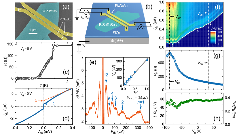
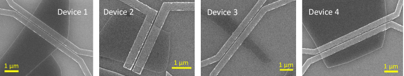
The TI-based JJs reported here are fabricated on bulk-insulating BiSbTeSe2 flakes. A scanning electron microscope (SEM) image of a typical device is shown in Figure 1a as an example, and the device structure is schematically illustrated in Figure 1b. The flakes of BiSbTeSe2 were exfoliated from a bulk single crystal and then transferred onto degenerately-doped Si substrates having a 290-nm-thick SiO2 coating layer, which serves as the dielectric of the back gate. Flakes with a thickness of 20 nm or thinner were selected for device fabrication, so that the of the top surface can be controlled with the back gate. The JJ is defined by patterning two parallel Pt/Al/Au electrodes with a spacing to cover the full width of a selected flake; we call and the length and the width of the junction, respectively. Here the thin Pt layer works as a buffer layer to improve the transparency of Al/BiSbTeSe2 contacts, and the Au capping layer helps to prevent Al electrodes from oxidization in air. We have investigated four JJ devices (denoted devices 1 – 4) with essentially the same design (see Supporting Figure S1 for their pictures). The dimensions of all the devices are shown in Table S1 of the Supporting Information. The measurements were performed in a pseudo-four-wire configuration as illustrated in Figure 1b, by using both ac and dc techniques (see detailed descriptions at the end).
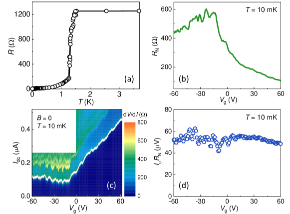
The temperature dependence of the junction resistance in device 1 is shown in Figure 1c. Superconducting transitions occur successively upon cooling: First, a sharp drop in is observed at K, and then a broad transition continues down to 750 mK, below which the junction reaches a zero-resistance state. The first transition corresponds to the superconducting transition of Al electrodes, and the second transition is associated with the onset of Josephson coupling between the two Al electrodes.
A typical - curve of device 1 measured at = 0 V is plotted in Figure 1d. For an applied dc current smaller than the critical current A, the junction is in the superconducting state and the measured voltage remains zero. When exceeds , a finite starts to develop, and the junction is driven into a resistive state. However, due to quasiparticle processes such as multiple Andreev reflection, the - curve is nonlinear at low . The linearity in the - curve gradually recovers when goes beyond ; the inverse of the slope in this linear region gives a normal-state resistance . An excess current A is obtained by linearly extrapolating the - curve from the linear region to V, as illustrated in Figure 1c. Based on the Octavio-Tinkham-Blonder-Klapwijk theory OTBK-theory-Octavio , the transparency of the Al/Pt/BiSbTeSe2 contact can be estimated from the values of and OTBK-theory-Flensberg , and is obtained for device 1. (see Supporting Information for details).
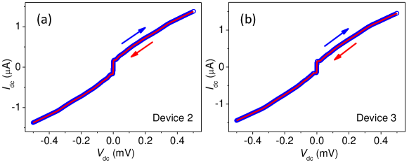
The - curves of our JJs show no hysteretic behaviour; the values of obtained in up- and down-sweeps are identical. Such non-hysteretic -s are usually seen in overdamped JJs. The Stewart-McCumber parameter of device 1 is estimated to be , where is the shunt capacitance between the two Al electrodes. Similar values of are obtained for other devices (Supporting Information). Such intermediate values of indicate that our JJs lie in the region between the overdamped and underdamped limits. According to numerical calculations, JJs in such a region show non-hysteretic - characteristics similar to those of underdamped JJs TI-JJ-exp-GoldhaberGordon ; JJ-book-Likharev , which is consistent with our observation.
Sub-harmonic peaks at are often observed in the vs curves of voltage-biased JJs which satisfy . Here, is the superconducting energy gap, is the peak index and is the inelastic scattering length of the normal metal. Such sub-harmonic features are associated with multiple Andreev reflection (MAR) processes MAR-theory-Klapwijk taking place in the channel of a JJ. In the past, the MAR peaks have been observed in a variety of TI-based JJs TI-JJ-Samarth ; TI-JJ-exp-Molenkamp ; TI-JJ-exp-Chen .
In the present experiment, clear MAR peaks were seen in the vs curves of all four devices. A typical curve measured in device 2 is plotted in Figure 1e with assigned peak indices. The assignments of are confirmed by the linear relation between and illustrated in the inset of Figure 1e. A linear fit to the data gives eV, consistent with the superconducting gap reported for Al in the literature TI-JJ-exp-GoldhaberGordon .
A key feature in Figure 1e is the presence of high-index conductance peaks reaching = 12, indicating that the inelastic scattering length in BiSbTeSe2 exceeds (= 840 nm), which is longer than what was reported for previous TI-based JJs TI-JJ-exp-GoldhaberGordon . Nevertheless, such a long is consistent with previous results of Aharonov-Bohm oscillations observed in square-ring interferometers based on Bi2Se3 flakes AB-effect-LiLu . In addition, the presence of high-index peaks also indicates a relatively high transparency of the Al/BiSbTeSe2 contacts. Numerical calculations MAR-peak-index-Yeyati ; MAR-peak-index-Bardas show that high-index features of MAR become the most visible when takes a relatively high value of around , while they disappear in both transparent () and tunneling () limits, which is consistent with our estimate of = 0.83 for device 2.
The amplitude of the conductance peak at is expected to decay with increasing , because the probability of MAR processes generally decreases with . However, in our experiment, the peak shows an amplitude much larger than those of other peaks. The origin of the larger-than-expected amplitude of peak is not clear and the reason for the absence of peaks for is unknown. Nevertheless, similar MAR phenomena have been seen in previous experiments on TI-based JJs by Jauregui et al. TI-JJ-exp-Chen and on Ge/Si-nanowire-based JJs by Xiang et al. Xiang2006 .
As-grown BiSbTeSe2 single crystals are bulk-insulating, with located slightly below the Dirac point BSTS2-sato . However, due to the unintentional doping introduced during the exfoliation and device fabrication processes, in our samples is shifted into the -type region. Nevertheless, the top-surface Fermi level of our devices can be tuned by the back-gate voltage to the Dirac point, thanks to the small thickness (18 nm) of the TI flakes used here; in the following, denotes the value needed to bring the Fermi level to the Dirac point. For a detailed analysis of the single-gate control of the Fermi levels of two surfaces involving a capacitive coupling, see Ref. 35.
The normal-state resistance vs curve of device 1 is plotted in Figure 1g. Here, was measured by suppressing the superconductivity of Al with a magnetic field; note that and are not exactly the same, which probably indicates that the contact resistance is very sensitive to the magnetic field. The position of the Dirac point V is determined by the peak in this curve, while the position of the conduction band bottom is estimated by using V, where is the two-dimensional carrier density in BiSbTeSe2 when reaches the bottom of the conduction band, and is the capacitance per unit area of the back gate (see Supporting Information for details).
Figure 1f shows the colour mapping of in device 1 scanned in the vs plane. The critical current is depicted by the white band at the edge of the superconducting region in deep blue colour. A finite of 92 nA is observed at the Dirac point. In the -type region where , increases sharply with increasing . However, in the -type region where , saturates when decreases. In device 2 where can be tuned deeper into the -type region, we found that actually increases slowly with decreasing in the -type region, although the rate of increase is very low (see Supporting Figure S2c). In the past, similar asymmetric behavior was also reported in TI-based JJs TI-JJ-exp-Mason ; TI-JJ-exp-Chen and graphene Graphine-JJ-exp-Geim , and it was speculated that this behaviour is caused by the - junctions formed between the gated junction channel and the areas under the SC contacts.
The product of device 1 is calculated as a function of using the data in Figures 1f and 1g, and shown in Figure 1h. The product is almost independent of except for the region near the Dirac point. When approaches the Dirac point from the -type region, presents a minimum at around V. Similar behavior in was observed with less clarity in device 2 (see Supporting Figure S2d). The origin of this minimum is not clear. Most importantly, device 1 shows the ratio of up to 0.37, which is among the largest values reported in the literature TI-JJ-exp-Brinkman ; TI-JJ-exp-LiLu ; TI-JJ-exp-GoldhaberGordon ; TI-JJ-exp-Molenkamp ; TI-JJ-exp-Mason ; TI-JJ-exp-Lee ; TI-JJ-exp-Lombardi ; TI-JJ-exp-Brinkman2 ; TI-JJ-exp-Juelich ; TI-JJ-exp-Chen , again proving the high transparency of the Al/BiSbTeSe2 contacts realized in the present work.
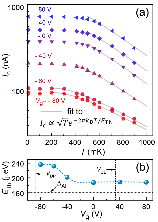
The temperature dependence of was measured at various values, as plotted in Figure 2a. With decreasing , first increases exponentially and then saturates. The step-like increase in at low temperature reported in a recent work on TI-based JJs using Nb electrodes TI-JJ-exp-Juelich was not observed in our devices. A fit to in the high-temperature range allows us to extract the Thouless energy () at various TI-JJ-exp-Lombardi ; CPR-review-Golubov ; here, is the average diffusion constant of supercurrent-carrying electrons and is the length of the JJ.
The values obtained from the fittings are plotted in Figure 2b as a function of . It is noteworthy that remains unchanged when moves through the bottom of the conduction band at . In other words, the presence of bulk carriers does not change the average of the supercurrent-carrying electrons. Since of bulk carriers is expected to be much smaller than that of the surface electrons, the unchanged suggests that the supercurrent is mainly carried by the surfaces states even when is located inside the conduction band. This is in agreement with the conclusions in previous studies on planar TI-based JJs TI-JJ-exp-Brinkman ; TI-JJ-exp-Mason , but contradicts the results obtained in Pb-Bi2Se3-Pb JJs fabricated along the -direction of Bi2Se3 flakes TI-JJ-exp-LiLu . As approaches the Dirac point from the -type region, starts to increase, indicating an increase in of the surface electrons. Such an enhancement of around the Dirac point is probably due to the smaller phase space available for scattering. In addition, the extracted is comparable to in the entire range of , indicating that our junctions lie on the boundary between the short- and long-junction limit, similar to what was previously reported in Al-Bi2Se3-Al junctionsTI-JJ-exp-Lombardi .
To determine the regime to which our JJs belong, it is important to estimate several characteristic lengths. As discussed above, the lower boundary of the inelastic scattering length is estimated from the MAR results to be = 840 nm. The superconducting coherence length in BiSbTeSe2 is given by . With = 70 nm measured in the SEM image, eV obtained from the MAR data, and = 187 – 236 eV extracted from the curves, we obtain nm. The mean free path of the supercurrent-carrying surface electrons can be calculated by using and , where m/s is the Fermi velocity of the surface states BSTS2-sato , and one obtains = 5.1 – 6.4 nm, which is much shorter than the previously reported value nm in Bi1.5Sb0.5Te1.7Se1.3 bulk crystals BSTS-transport-Ando . We tentatively attribute the short in the BiSbTeSe2 flakes to the surface disorder introduced in the device fabrication process. While a short might seem a disadvantage for quantum computing, the readout of Majorana qubits can be performed without relying on ballistic transport Schrade . The characteristic lengths estimated above point to the relation , which indicates that our JJs are diffusive junctions () in the intermediate region between the short- and long-junction limit ().
For JJs satisfying , the ratio is expected to be of order 1 at K JJ-review-Likharev . However, in reality, the measured values of are usually much smaller than the theoretical expectation due to the existence of resistive shunt channels or limited SC contact transparency TI-JJ-exp-Lombardi . The ratio found in previous studies on TI-based JJs ranges between 0.01 and 0.31, all smaller than the ratio of 0.37 observed in device 1, indicating that the quality of our TI-based JJs is among the best in terms of bulk-insulating property and contact transparency.
For a trivial JJ with a homogeneous current distribution, the vs relation is expected to exhibit a so-called Fraunhofer pattern described by
| (1) |
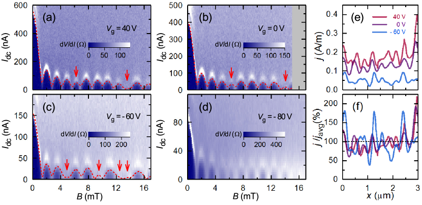
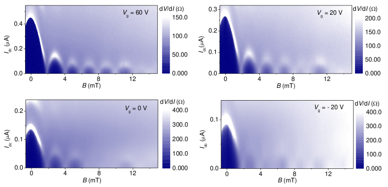
where is the critical current at , is the flux threading through the junction channel and is the flux quantum. To elucidate the behaviour of our JJs, the data were measured as a function of and at various corresponding to the positions from inside the conduction band to near the Dirac point. The patterns of device 1 are shown in Figures 3a–3d. All the observed patterns are essentially Fraunhofer-like, but bear anomalous features that deviate from a standard Fraunhofer pattern. They include: (i) an average period mT, which is about three times smaller than the expected period mT estimated from the junction area , where (nm) is the London penetration depth of bulk Al, and (ii) missing or significantly suppressed lobes which cannot be described by the formula for the Fraunhofer pattern.
Anomalous features in the Fraunhofer patterns have been reported for TI-based JJs in some of the previous works TI-JJ-exp-GoldhaberGordon ; TI-JJ-exp-Lee ; Suominen ; Bocquillon . There was an attempt to explain the smaller-than-expected by a phenomenological model involving quantized Majorana modes TI-JJ-exp-GoldhaberGordon . However, in the present case, it may partly be explained by a small 2D superfluid density (and hence longer effective ) in the 30-nm-thick Al electrodes which are thinner than the bulk . Also, it has been noted that the small can be explained by the flux focusing effect TI-JJ-exp-LiLu , which is commonly seen in planar JJs flux-focusing-Rosenthal . Due to the diamagnetism of a SC, the magnetic field near the SC electrodes is distorted, and half of the magnetic flux expelled from the SC electrodes is compressed into the junction; this effect may be quantified in terms of an extended effective junction area , where is the effective junction length considering the flux focusing ( and are the widths of the left and right SC electrodes). Taking nm and nm for device 1, we obtain mT, which is close to the observed average period mT. Therefore, in the following, we use instead of for the reconstruction of the patterns.
Regarding the origin of the other feature, i.e. missing lobes in the Fraunhofer pattern, this has been left unexplained in the literature TI-JJ-exp-Lee ; Suominen ; Bocquillon . Theoretically, an irregular pattern could be generated by (i) a non-sinusoidal current phase relation or (ii) an inhomogeneous supercurrent distribution in the JJ. In the past, much attention has been paid to the first possibility. For instance, it was predicted that the formation of 1D Majorana modes in a TI-based JJ gives rise to an pattern featuring a non-zero first minimum, deviating from a standard Fraunhofer pattern LiangFu-2013 . It was also predicted that the periodicity due to Majorana zero-modes leads to a suppression of the odd-numbered (1st, 3rd, 5th, etc.) lobes in the Fraunhofer patttern Baxevanis .
However, these theoretical possibilities do not really explain the disappearance of some particular lobes, and one had better consider the second possibility to understand the irregular patterns observed in our TI-based JJs. We set out to reconstruct the anomalous Fraunhofer patterns by considering an inhomogeneous supercurrent distribution along the width of the junction. The experimental data of , extracted from the data as the onset of rapid increase, are fitted by using a Monte Carlo algorithm to optimize the form of based on the maximum entropy method (see detailed descriptions at the end), which has not been applied to the present problem; this method removes the constraint of the standard Dynes-Fulton-type analysis Dynes1971 ; Allen2016 ; Zappe1975 ; Nesher1997 ; Hui2014 and allows to identify any form of inhomogeneous supercurrent distribution. In Figure 3e we plot for three values the obtained forms of , which reproduce all the main features in the patterns as shown with red dashed lines in Figures 3a–3c. In the normalized plot of shown in Figure 3f, one can see that the relative magnitude of the fluctuations is enhanced at V, which is close to the Dirac point. The enhancement of at the edges seen in Figure 3f is probably due to the contribution of the side surfaces TI-JJ-exp-Lee which also contain topological surface states. We did not perform a fitting of the data for V, because the values at this could not be reliably extracted due to the absence of true supercurrents in magnetic fields of only a few mT.
We note that the curves presented in Figure 3e are not the unique solutions which give good fittings to the data. This is partly because of the lack of the phase information in this inverse problem, but also because of the trade-off between the degree of fitting and the smoothness of the solution. Nevertheless, it is clear from the present analysis that the existence of an inhomogeneous is sufficient for causing the observed anomalous Fraunhofer patterns, most notably missing lobes.
An inhomogeneous can be caused by various reasons. One possible reason is the fluctuations in the junction length due to the roughness of the edges of Al electrodes. Since the critical current depends exponentially on , for junctions with a short , even small fluctuations in could result in a notable variation in . Another possible reason is a position-dependent transparency of the Al/TI interface, which may arise from a granularity of the Al film. In addition, a possible variation of the surface carrier density due to charge puddles puddles-Breunig2017 may also be partially responsible for the inhomogeneous .
To conclude, we have established a highly promising fabrication technology for TI-based JJs, which allowed us to elucidate that the anomalous Fraunhofer patterns are essentially due to an inhomogeneous supercurrent distribution in the proximitized surface states. This technology and the quantitative understanding gained in this work would make it possible to fabricate an optimized device to nail down the signature of Majorana fermions in the proximitized TI surface in near future.
Growth of bulk BiSbTeSe2 crystals: The bulk BiSbTeSe2 single crystals were grown by melting high-purity (99.9999%) Bi, Sb, Te, and Se shots with the molar ratio of 1:1:1:2 in an evacuated quartz tube via a modified Bridgman method, following our established recipe reported in Ref. 24. The grown crystals typically have a domain size of several mm and are easily cleaved along the (111) plane.
Device fabrication: Ultrathin BiSbTeSe2 flakes are obtained by mechanical exfoliation of bulk single crystals on degenerately-doped Si/SiO2 wafers by a Scotch-tape technique. Promising flakes are initially identified under a laser microscope (Keyence VK-X200), and further characterized by atomic force microscopy. The flakes with an extremely smooth surface (without atomic terraces) are chosen for the fabrication of JJ devices using electron beam lithography. Previous studies on a similar bulk-insulating TI material have shown TI-JJ-exp-Brinkman2 that a very short junction channel (50 nm) is essential for realizing a sufficiently strong coupling between two SC electrodes to observe a Josephson supercurrent. To reliably fabricate short-channel junctions, we have developed our own recipe. A 160-nm-thick PMMA layer was spin coated and baked at 120∘C for 10 minutes. The reduced baking temperature ensures minimal unintentional doping due to creation of Se vacancies at elevated temperatures. The resist layer was exposed by a 25-kV electron beam. The width of the Al electrodes was kept around 400 nm to avoid vortex movements at finite magnetic fields in the superconducting state. To remove any resist residues in the contact areas after the development, the wafers were cleaned with oxygen plasma in a reactive-ion etching machine at 20 W for 7 s. Afterwards, the wafers were further cleaned in a HCl solution to remove any oxide layer in the contact areas. The metallization was carried out by sputtering 5-nm-thick Pt as buffer layer, followed by thermal evaporation of 30-nm-thick Al at the pressure of mbar. A 5-nm-thick Au layer was successively evaporated to protect the Al from oxidation, and the lift-off was done in warmed acetone.
Measurements: The devices were cooled in a dry dilution refrigerator (Oxford Instruments TRITON 200) with a base temperature of less than 10 mK. To reduce the electromagnetic noise, the electrical lines are equipped with RC-filters at room temperature and at the 4-K plate, along with additional RC and copper-powder filters at the mixing chamber plate. The junctions were electrically characterized by dc current-voltage (-) and differential resistance () measurements in a pseudo-four-probe configuration. For the measurement, an 18.6-Hz ac current with the amplitude of 1 nA was superimposed to a dc bias current. The magnetic-field dependence of the critical current (i.e. Fraunhofer pattern) was measured by performing the measurements while driving the superconducting magnet with a Keithley 2450 source meter.
Current density retrieval: For a JJ with a sinusoidal current-phase relation, the experimentally observed critical current is related to the modulus of the phase-dependent integration of the supercurrent density Dynes1971 ,
| (2) |
which allows to deduce information about the distribution of the current density and the phase difference within the junction. In the present case of a narrow JJ (i.e. , where is the Josephson penetration length), can be assumed to depend linearly on the spatial position along the junction and on the applied magnetic field ; namely, , where is the magnetic flux quantum and is the effective length of the JJ to take into account the flux focusing effect of the superconducting electrode of width flux-focusing-Rosenthal . This phase factor makes the integration to be effectively a Fourier transform from the coordinate to the coordinate. In general, the supercurrent density may depend on both the spatial coordinates and within the junction area; however, we restrict ourselves to the dependence on defined along the junction’s width , by considering the one-dimensional current density .
As the critical current does not contain information on the complex phase of the Fourier transform, but only on its modulus, the current density cannot be obtained unambiguously from the experimental data . In fact, there is an infinitely large number of current profiles that yield a similar . Most of previous reconstructions of the current distribution were essentially based on the Dynes-Fulton analysis Dynes1971 ; Allen2016 ; Zappe1975 ; Nesher1997 ; Hui2014 . Although the original Dynes-Fulton analysis utilized a relatively strong assumption that is an approximately even function Dynes1971 , some of the later attempts have relaxed this constraint Zappe1975 ; Nesher1997 ; Hui2014 . In this work, we perform a novel type of analysis based on the ideas of Dynes and Fulton, but without requiring any presumptions; specifically, we identify the most physical solution by using a maximum entropy method Jaynes . The outline of our fitting procedure is the following: First, we discretize into elements and initialize them to a value of . To ensure the agreement with the zero-field critical current, we keep to be fixed. Then we fit the data by maximizing the functional using a Monte Carlo algorithm. Here, is the square of the deviation from the experimental data taken at points , and the second term is the entropy of the normalized current distribution . The weighting factor tunes between a pure least-square fit for and an increasing contribution of the maximum entropy method for . A larger gives a better fitting, but the obtained current distribution tends to become unphysically peaky; more weighting of the entropy term makes the resulting current distribution to be smoother and more physical, even though becomes larger. In our analysis, the value of is initially set to , and we increase (decrease) it during the Monte Carlo steps when the iteration goes to the wrong direction, i.e., when becomes larger (smaller) than a given target value ; such a dynamical tuning of allows the square term to converge to while ensuring the resulting current distribution to be smooth. Still, the algorithm does not provide a single and unique solution for the current distribution, and the smoothness of the distribution depends on the choice of . To avoid over-fitting of the data, for each data set the maximal was chosen so that the calculated reproduces the absent lobes and the overall shape of the Fraunhofer pattern. Typically, the fits converged after about 50,000 steps. Each data set was processed about 100 times to check for the robustness of the fitting result, and we found that the obtained current distributions – save for mirror symmetry – resembled each other within a few percent of deviation. From these we pick the solution having the largest entropy and show it in Figure 3.
Author contributions: S.G., O.B. and F.Y contributed equally to this work and should be considered as co-first authors.
Acknowledgement: This project has received funding from the European Research Council (ERC) under the European Union’s Horizon 2020 research and innovation programme (grant agreement No 741121) and was also supported by DFG (CRC1238 “Control and Dynamics of Quantum Materials”, Projects A04 and B01). We thank D. Goldhaber-Gordon, A. Rosch, S. Trebst, and Y. Vinkler for helpful discussions. O.B. acknowledges the support from Quantum Matter and Materials Program at the University of Cologne funded by the German Excellence Initiative.
References
- (1) Fu, L.; Kane, C. L. Superconducting Proximity Effect and Majorana Fermions at the Surface of a Topological Insulator. Phys. Rev. Lett. 2008, 100, 96407.
- (2) Sato, M.; Ando, Y. Topological Superconductors: A Review. Rep. Prog. Phys. 2017, 80, 076501.
- (3) Hasan, M. Z.; Kane, C. L. Colloquium: Topological insulators. Rev. Mod. Phys. 2010, 82, 3045-3067.
- (4) Qi, X.-L.; Zhang, S.-C. Topological Insulators and Superconductors. Rev. Mod. Phys. 2011, 83, 1057-1110.
- (5) Ando, Y. Topological Insulator Materials. J. Phys. Soc. Jpn. 2013, 82, 102001.
- (6) Elliott, S. R.; Franz., M. Colloquium: Majorana Fermions in Nuclear, Particle, and Solid-State Physics. Rev. Mod. Phys. 2015, 87, 137-163.
- (7) Sarma, S. D.; Freedman, M.; Nayak, C. Majorana Zero Modes and Topological Quantum Computation npj Quantum Inf. 2015, 1, 15001.
- (8) Klapwijk, T. M. Proximity Effect from an Andreev Perspective. J. Supercond. Novel Magn. 2004, 17, 593-611.
- (9) Snelder, M.; Veldhorst, M.; Golubov, A. A.; Brinkman, A. Andreev Bound States and Current-Phase Relations in Three-Dimensional Topological Insulators. Phys. Rev. B 2013, 87, 104507.
- (10) Zhang, D.; Wang, J.; DaSilva, A. M.; Lee, J. S.; Gutierrez, H. R.; Chan, M. H. W.; Jain, J.; Samarth, N. Superconducting Proximity Effect and Possible Evidence for Pearl Vortices in a Candidate Topological Insulator. Phys. Rev. B 2011, 84, 165120.
- (11) Veldhorst, M.; Snelder, M.; Hoek, M.; Gang, T.; Guduru, V. K.; Wang, X. L.; Zeitler, U.; van der Wiel, W. G.; Golubov, A. A.; Hilgenkamp, H.; et al. Josephson Supercurrent through a Topological Insulator Surface State. Nat. Mater. 2012, 11, 417-421.
- (12) Qu, F.; Yang, F.; Shen, J.; Ding, Y.; Chen, J.; Ji, Z.; Liu, G.; Fan, J.; Jing, X.; Yang, C.; et al. Strong Superconducting Proximity Effect in Pb-Bi2Te3 Hybrid Structures. Sci. Rep. 2012, 2, 339.
- (13) Williams, J. R.; Bestwick, A. J.; Gallagher, P.; Hong, S. S.; Cui, Y.; Bleich, A. S.; Analytis, J. G.; Fisher, I. R.; Goldhaber-Gordon, D. Unconventional Josephson Effect in Hybrid Superconductor-Topological Insulator Devices. Phys. Rev. Lett. 2012, 109, 56803.
- (14) Galletti, L.; Charpentier, S.; Iavarone, M.; Lucignano, P.; Massarotti, D.; Arpaia, R.; Suzuki, Y.; Kadowaki, K.; Bauch, T.; Tagliacozzo, A.; et al. Influence of Topological Edge States on the Properties of Al/Bi2Se3/Al Hybrid Josephson Devices. Phys. Rev. B 2014, 89, 134512.
- (15) Schüffelgen, P.; Rosenbach, D.; Li, C.; Schmitt, T.; Schleenvoigt, M.; Jalil, A. R.; Kölzer, J.; Wang, M.; Bennemann, B.; Parlak, U.; et al. Boosting Transparency in Topological Josephson Junctions via Stencil Lithography. 2017, arXiv:1711.01665 [cond-mat.supr-con].
- (16) Oostinga, Jeroen B.; Maier, Luis; Schüffelgen, Peter; Knott, Daniel; Ames, Christopher; Brüne, Christoph; Tkachov, Grigory; Buhmann, Hartmut; Molenkamp, Laurens W. Josephson Supercurrent through the Topological Surface States of Strained Bulk HgTe. Phys. Rev. X 2013, 3, 21007.
- (17) Cho, S.; Dellabetta, B.; Yang, A.; Schneeloch, J.; Xu, Z.; Valla, T.; Gu, G.; Gilbert, M. J.; Mason, N. Symmetry Protected Josephson Supercurrents in Three-Dimensional Topological Insulators. Nat. Commun. 2013, 4, 1689.
- (18) Lee, J.H.; Lee, G.H.; Park, J.; Lee, J.; Nam, S.G.; Shin, Y.S.; Kim, J.S.; Lee, H.J. Local and Nonlocal Fraunhofer-like Pattern from an Edge-Stepped Topological Surface Josephson Current Distribution. Nano Lett. 2014, 14, 5029-5034.
- (19) Snelder, M.; Molenaar, C. G.; Pan, Y.; Wu, D.; Huang, Y. K.; de Visser, A.; Golubov, A. A.; van der Wiel, W. G.; Hilgenkamp, H.; Golden, M. S.; et al. Josephson Supercurrent in a Topological Insulator without a Bulk Shunt. Supercond. Sci. Technol. 2014, 27, 104001.
- (20) Wiedenmann, J.; Bocquillon, E.; Deacon, R. S.; Hartinger, S.; Herrmann, O.;Klapwijk, T. M.; Maier, L.; Ames, C.; Brüne, C.; Gould, C.; et al. -periodic Josephson Supercurrent in HgTe-based Topological Josephson Junctions. Nat. Commun. 2016, 7, 10303.
- (21) Jauregui, L. A.; Kayyalha, M.; Kazakov, A.; Miotkowski, I.; Rokhinson, L. P.; Chen, Y. P.; Gate-tunable Supercurrent and Multiple Andreev Reflections in a Superconductor-Topological Insulator Nanoribbon-Superconductor Hybrid Device. Appl. Phys. Lett. 2018, 112, 093105.
- (22) Bocquillon, E.; Deacon, R. S.; Wiedenmann, J.; Leubner, P.; Klapwijk, T. M.; Brüne, C.; Ishibashi, K.; Buhmann, H.; Molenkamp, L. W. Gapless Andreev Bound States in the Quantum Spin Hall Insulator HgTe. Nat. Nanotechnol. 2017, 12, 137-143.
- (23) Krogstrup, P.; Ziino, N. L. B.; Chang, W.; Albrecht, S. M.; Madsen, M. H.; Johnson, E.; Nygård, J.,;Marcus, C. M.; Jespersen, T. S. Epitaxy of Semiconductor-Superconductor Nanowires. Nat. Mater. 2015, 14, 400-406.
- (24) Ren, Z.; Taskin, A. A.; Sasaki, S.; Segawa, K.; Ando, Y. Optimizing Bi2-xSbxTe3-ySey Solid Solutions to Approach the Intrinsic Topological Insulator Regime. Phys. Rev. B 2011, 84, 165311.
- (25) Klapwijk, T. M.; Blonder, G. E.; Tinkham, M. Explanation of Subharmonic Energy Gap Structure in Superconducting Contacts. Physica B+C 1982, 109, 1657-1664.
- (26) Suominen, H. J.; Danon, J.; Kjaergaard, M.; Flensberg, K.; Shabani, J.; Palmstrøm, C. J.; Nichele, F.; Marcus, C. M. Anomalous Fraunhofer Interference in Epitaxial Superconductor-Semiconductor Josephson Junctions. Phys. Rev. B 2017, 95, 035307.
- (27) Octavio, M.; Tinkham, M.; Blonder, G. E.; Klapwijk, T. M. Subharmonic Energy-Gap Structure in Superconducting Constrictions. Phys. Rev. B 1983, 27, 6739.
- (28) Flensberg, K.; Hansen, J. B.; Octavio, M. Subharmonic Energy-Gap Structure in Superconducting Weak Links. Phys. Rev. B 1988, 38, 8707.
- (29) Likharev, K. K. Dynamics of Josephson Junctions and Circuits; Gordon and Breach Science Publishers, 1986.
- (30) Qu, F.;Yang, F.;Chen, J.;Shen, J.;Ding, Y.;Lu, J.;Song, Y.;Yang, H.;Liu, G.;Fan, J.; et al. Aharonov-Casher Effect in Bi2Se3 Square-Ring Interferometers. Phys. Rev. Lett. 2011, 107, 16802.
- (31) Cuevas, J. C.; Martin-Rodero, A.; Yeyati, A. L. Hamiltonian Approach to the Transport Properties of Superconducting Quantum Point Contacts. Phys. Rev. B 1996, 54, 7366.
- (32) Averin, D.; Bardas, A. ac Josephson Effect in a Single Quantum Channel. Phys. Rev. Lett. 1995, 75, 1831.
- (33) Xiang, J.; Vidan, A.; Tinkham, M.; Westervelt, R. M.; Lieber, C. M., Ge/Si nanowire mesoscopic Josephson junctions. Nature Nanotech. 2006, 1, 208.
- (34) Arakane, T.; Sato, T.; Souma, S.; Kosaka, K.; Nakayama, K. ; Komatsu, M.; Takahashi, T.; Ren, Z.; Segawa, K.; Ando, Y. Tunable Dirac Cone in the Topological Insulator Bi2-xSbxTe3-ySey. Nat. Commun. 2012, 3, 636.
- (35) Yang, F.; Taskin, A. A.; Sasaki, S.; Segawa, K.; Ohno, Y.; Matsumoto, K.; Ando, Y., Dual-Gated Topological Insulator Thin-Film Device for Efficient Fermi-Level Tuning. ACS Nano 2015, 9, 4050-4055.
- (36) Ben Shalom, M.; Zhu, M. J.; Fal’ko, V. I.; Mishchenko, A.; Kretinin, A. V.; Novoselov, K. S.; Woods, C. R.; Watanabe, K.; Taniguchi, T.; Geim, A. K.; et al. Quantum Oscillations of the Critical Current and High-Field Superconducting Proximity in Ballistic Graphene. Nat. Phys. 2016, 12, 318-322.
- (37) Rosenthal, P. A. et al. Flux Focusing Effects in Planar Thin-Film Grain-Boundary Josephson Junctions. Appl. Phys. Lett. 1991, 59, 3482-3484.
- (38) Potter, A. C.; Fu, L. Anomalous Supercurrent from Majorana States in Topological Insulator Josephson Junctions. Phys. Rev. B 2013, 88, 121109.
- (39) Baxevanis, B., Ostroukh, V. P.; Beenakker, C. W. J. Even-odd Flux Quanta Effect in the Fraunhofer Oscillations of an Edge-Channel Josephson Junction. Phys. Rev. B 2015, 91, 041409.
- (40) Breunig, O.; Wang, Z.; Taskin, A. A.; Lux, J.; Rosch, A.; Ando, Y. Gigantic Negative Magnetoresistance in the Bulk of a Disordered Topological Insulator. Nat. Commun. 2017, 8, 15545.
- (41) Golubov, A. A.; Kupriyanov, M. Y.; Il Ichev, E. The Current-Phase Relation in Josephson Junctions. Rev. Mod. Phys. 2004, 76, 411.
- (42) Taskin, A. A.; Ren, Z.; Sasaki, S.; Segawa, K.; Ando, Y. Observation of Dirac Holes and Electrons in a Topological Insulator. Phys. Rev. Lett. 2011, 107, 016801.
- (43) Schrade, C.; Fu, L. Majorana Superconducting Qubit. 2018, arXiv:1803.01002 [cond-mat.mes-hall].
- (44) Likharev, K. K. Superconducting Weak Links. Rev. Mod. Phys. 1979, 51, 101.
- (45) Dynes, R. C.; Fulton, T. A. Supercurrent Density Distribution in Josephson Junctions. Phys. Rev. B 1971, 3, 3015.
- (46) Allen, M. T.; Shtanko, O.; Fulga, I. C.; Akhmerov, A. R.; Watanabe, K.; Taniguchi, T.; Jarillo-Herrero, P.; Levitov, L. S.; Yacoby, A. Spatially Resolved Edge Currents and Guided-Wave Electronic States in Graphene. Nat. Phys. 2016, 12, 128.
- (47) Zappe, H. H. Determination of the Current Density Distribution in Josephson Tunnel Junctions. Phys. Rev. B 1975, 11, 2535.
- (48) Nesher, O.; Ribak, E. N. Retrieval of Critical Current Distribution in Small Josephson Junctions. Appl. Phys. Lett. 1997, 71, 1249-1251.
- (49) Hui, H.-Y.; Lobos, A. M.; Sau, J. D.; Das Sarma, S. Proximity-induced Superconductivity and Josephson Critical Current in Quantum Spin Hall Systems. Phys. Rev. B 2014, 90, 224517.
- (50) Jaynes, E.T. Information Theory and Statistical Mechanics. Phys. Rev. 1957, 106, 620-630.
Supporting Information
1. SEM images of all devices
The SEM images of all four devices are shown in Figure S1.
2. Characteristic parameters of all devices
Characteristic parameters of all four devices are listed in Table S1. Here, denotes the normal-state resistance measured by applying a magnetic field or a large excitation current , while is the normal-state resistance extracted from - curves. Since is obtained with Al in the normal-conducting state one may naively expect that . Yet, the opposite is observed, which may be explained by a change of the density of states in the TI due to the proximity effect Gueron-2012 .
| No. | (nm) | (m) | (nm) | (A) | (A) | () | () | (V) | (V) | ||||
| 1 | 70 | 2.9 | 18 | 0.39 | 0.94 | 141 | 187 | 55 | 73 | 0.34 | 0.45 | 0.99 | 0.77 |
| 2 | 70 | 2.2 | 17 | 0.15 | 0.42 | 348 | 536 | 52 | 96 | 0.33 | 0.60 | 2.51 | 0.83 |
| 3 | 78 | 1.0 | 13 | 0.16 | 0.51 | - | 493 | - | 78 | - | 0.49 | 1.77 | 0.86 |
| 4 | 79 | 5.6 | 21 | 0.51 | 1.41 | - | 75 | - | 38 | - | 0.24 | 0.23 | 0.65 |
3. Characterization of device 2
Several Al-BiSbTeSe2-Al Josephson junctions were measured down to low temperatures, and all investigated devices showed consistent behaviour. In Figure S2, we present a full characterization of device 2. Essentially all the results of device 1 are reproduced in device 2, except that the of device 2 is much closer to the Dirac point at .
Similar to device 1, a two-step transition was seen in the cooling curve of device 2. The sharp transition at K is associated with the superconducting of Al, and the broad transition occurring subsequently reflects the development of Josephson coupling. Due to the low carrier density at , device 2 reaches zero resistance at a lower compared to device 1 (presented in the main text). The Dirac point of device 2 is located at V (which we define as ), and the can be tuned deeply beneath the Dirac point by applying a large negative , which enables us to investigate the vs relation in a wide range of the -type region. The measured curve is illustrated by the white band in Figure S2(c). One can see that in the -type region where V, the of device 2 actually increases slowly with decreasing . The product of device 2 plotted in Figure S2(d) shows a behavior similar to that of device 1, although the minimum (at V) is less clear.
4. Fraunhofer patterns of device 2 at various
In Figure S3, we present the 2D colour maps of the data in the vs plane measured in devices 2. Irregular Fraunhofer patterns with suppressed or missing lobes were observed in the entire range of the gate voltage. As approaches the Dirac point, the Fraunhofer pattern becomes blurred, and the oscillations of are only barely visible. This is presumably because the Josephson coupling is weakened at the Dirac point due to a low carrier density, and consequently the zero-resistance state is more prone to the thermal perturbation caused by electromagnetic noise.
5. Estimation of Stewart-McCumber parameter
Figure S4 shows the - curves of device 2 and device 3 measured in both forward and backward sweep directions. It is clear that the dc - characteristics are non-hysteretic. In the RCSJ model, such behaviour is expected for overdamped Josephson junctions in which the Stewart-McCumber parameter () is much smaller than unity ( is the shunt capacitance of the junction). To calculate the of our junctions, we estimated the shunt capacitance by considering the two capacitors forming between the two Pt/Al/Au contact pads and the conductive Si substrate via the 290-nm-thick SiO2 dielectric layer. It should be noted that these two capacitors are connected in series. Using the dielectric constant = 3.9 for SiO2 and the areas of the contact pads of the devices, we estimate fF. The shunt capacitance originating from the direct capacitive coupling between the two closely spaced Al electrodes at the junction is estimated to be roughly three orders of magnitude smaller than this and hence is safely neglected.
Using the estimated values of , we obtain in different devices (see Table S1). In the framework of the RCSJ-model, these junctions are at the boundary between the underdamped () and overdamped () regimes. In the literature, a previous study by Goldhaber-Gordon’s group reported TI-based Josephson junctions in this regime, and a non-hysteretic behaviour similar to ours was observed Williams-PRL-2012 . The numerical calculation for junctions in this regime also gave similar non-hysteretic results JJ-book-Likharev . Therefore, the absence of hysteresis in the dc - characteristics of our devices is consistent with their estimated values.
6. Estimation of the transparency of Al-BiSbTeSe2 contacts
The transparency of our Al-BiSbTeSe2 superconducting contacts were estimated from the values of and by using the Octavio-Tinkham-Blonder-Klapwijk theory OTBK-1983 ; OTBK-1988 . Here, and are the excess current and the normal-state resistance extracted from the - characteristics of the Josephson junctions, as defined in the main text. To identify , the dc - curves were measured to a high bias beyond , where eV is the superconducting gap of Al. The linear part of the high-bias - curve was extrapolated to and the intercept on the axis gives . The value was calculated as the inverse slope at high bias (i.e. ). The value of was obtained from the multiple Andreev reflection peaks as discussed in the main text. In Ref. 5, the normalized excess current / was numerically calculated as a function of the barrier strength , which is directly related to the transparency via . Using the given relation between / and , we estimated in our devices, as listed in Table S1.
7. Estimation of
Considering the contributions from both top and bottom surfaces, the total two-dimensional carrier density coming from the topological surface states in a ultra-thin sample is approximately given by
According to the ARPES results BSTS2-2012 , the conduction band bottom of BiSbTeSe2 is located at eV (measured from the Dirac point), and the Fermi wave vector of the surface states at this energy, , is about 0.076 Å-1. This gives cm-2.
The gate voltage required to tune from the Dirac point to the conduction band bottom is given by (. Here, nF/cm2 is the capacitance per unit area of the back gate, with and nm being the dielectric constant and the thickness of the SiO2 dielectric layer, respectively. With these values, we obtain V. For V in device 1 shown in the main text, one obtains V.
8. Applications of the maximum entropy fitting method
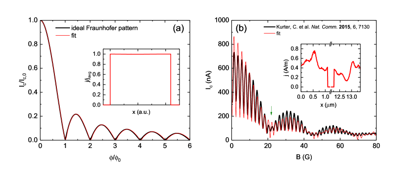
The presented anomalous Fraunhofer patterns have been analyzed using an advanced fitting scheme which is based on the maximum entropy principle. As a sanity check we applied the algorithm to an ideal pattern of a junction with a homogeneous current distribution given by , where and is the flux through the junction. First, we initialized the current distribution to random numbers and then applied the same algorithm used to describe the anomalous patterns in the main text. Both the good fit to as well as the flatness of the reconstructed current distribution (Figure S5(a)) show that the fluctuating current distribution extracted in the main text is neither due to over-fitting of the data, nor an artifact, but the most physical distribution explaining the experimental data.
We also applied the method to published data of SQUID oscillations measured from topological insulator Josephson junctions Kurter-2015 which have been argued by the authors to contain signatures of majorana bound states in the form of lifted SQUID nodes. To model the SQUID oscillations using our single junction fitting scheme, we forced the current distribution to be zero in the interval . Here, is the width of the individual junctions and represents the effective SQUID area with the effective length of the junctions. From the fit shown in Figure S5(b), we obtain , , and . These values are consistent with the observed oscillation period and with the device geometry, taking into account the effect of magnetic flux focusing. The reconstructed current density (inset of Figure S5(b)) shows moderate, yet finite spatial fluctuations whose amplitude and frequency are comparable to those discussed for our device in the main text. While the overall shape of the SQUID oscillations is well captured by our modeling, the lifting of the critical current close to the envelope’s first node (marked by an arrow) cannot be fully accounted for. Even the tuning of the algorithm from maximum entropy towards least-square fitting does not improve the fit in this data range, which opens a room for discussing more involved mechanisms for the observed node lifting.
References
- (1) Guéron, S.; Pothier, H.; Birge, N. O.; Esteve, D.; Devoret, M. H. Unconventional Josephson effect in hybrid superconductor-topological insulator devices. Phys. Rev. Lett. 2012, 77, 3025.
- (2) Williams, J. R.; et al. Unconventional Josephson effect in hybrid superconductor-topological insulator devices. Phys. Rev. Lett. 2012, 109, 56803.
- (3) Likharev, K. K. Dynamics of Josephson junctions and circuits (Gordon and Breach Science Publishers, 1986).
- (4) Octavio, M.; et al. Subharmonic energy-gap structure in superconducting constrictions. Phys. Rev. B 1983, 27, 6739.
- (5) Flensberg, K.; Hansen, J. B.; Octavio, M. Subharmonic energy-gap structure in superconducting weak links. Phys. Rev. B 1988, 38, 8707.
- (6) Arakane, T.; et al. Tunable Dirac cone in the topological insulator Bi2-xSbxTe3-ySey. Nat. Comm. 2012, 3, 636.
- (7) Kurter, C.; Finck, A. D. K.; Hor, Y. S.; van Harlingen, D. J. Evidence for an anomalous current–phase relation in topological insulator Josephson junctions. Nat. Comm. 2015, 6, 7130.