It has been proposed that a line junction between spiral magnet and superconductor or between ferromagnet and superconductor with Rashba spin-orbital coupling can produce Majorana zero mode (MZM) at the ends of the line. However, a strong magnetic exchange coupling between the magnetic atoms and the superconductor (about half of the bandwidth of the superconductor) is needed to obtain MZM. Here, we design devices to reduce the needed magnetic exchange coupling. In the first proposal, we cover a very narrow -wave superconducting wire formed by a monolayer film or a layered material (such as FeSe or FeSe monolayer on SrTiO3) with isolated magnetic atoms. In our second proposal, we place a line of isolated magnetic ions on a monolayer superconductor or a layered superconductor (such as FeSe). We show that, in the above devices, a spiral magnetic order will develop spontaneously to produce a 1D -wave topological superconductor with a sizable gap (above 1/2 of the parent superconducting gap), even for a weak magnetic exchange coupling (less than 1/10 of the bandwidth). The topological superconductor has MZM at ends of the wire.
Realizing Majorana zero mode with a stripe of ionized and isolated magnetic atoms on a layered superconductor
Introduction: Topological order Wen (1995) describes gapped phases of quantum matter at zero temperature that are robust against any perturbations (include those that break all the symmetries). For fermion systems, the simplest topological order is the so-called invertible topological order (iTO),Kong and Wen (2014); Freed (2014) such as 2D integer quantum Hall states von Klitzing et al. (1980), as well as 1D -wave Johnson and McCoy (1971); Kitaev (2001) and 2D -wave topological superconductors (TSC).Senthil et al. (1999); Read and Green (2000) The iTOs have no non-trivial bulk topological excitations. Their non-trivialness is reflected by their boundary states.
For example, the 1D -wave TSC chain of length has a 2-fold topological degeneracy in many-body energy levels. (A topological degeneracy is a non-exact degeneracy with splitting as sample size . Such a non-exact degeneracy is robust against any perturbations that can break any symmetry.Wen and Niu (1990)) The topological degeneracy can be used as logical qubits in topological quantum computing.Kitaev (2003) Since the 2-fold topological degeneracy comes from the two ends of the chain (there is no degeneracy for a -wave superconducting ring), each end carries degrees of freedom of one-half of a qubit: the Hilbert space for degrees of freedom at one end has a non-integer dimension (which is called the quantum dimension)! The emergence of non-integer degrees of freedom is a unique character of topological ordersWen (1991); Moore and Read (1991).
If the fermions in the chain are non-interacting, then the 2-fold topological degeneracy of the chain can be explained by the two Majorana zero modes (MZM) Read and Green (2000); Ivanov (2001) at the two ends of the chain.Johnson and McCoy (1971); Kitaev (2001) In this case, the non-integer degrees of freedom correspond to a Majorana zero mode. However, for interacting fermions, there are no single particle levels and no MZMs. In this case, we cannot regard the 2-fold topological degeneracy in terms of MZMs.


(a)
(b)
(c)
(d) (e)
There are many proposals to realize the 1D TSC. One class is to use a line junction between an -wave superconductor and a metallic quantum wire with spin-orbital coupling, in an external magnetic field or in the presence of magnetic moments in the metallic wire.Sau et al. (2010); Oreg et al. (2010); Potter and Lee (2012); Klinovaja et al. (2012); Kim et al. (2014) In this class of devices, the active electrons in the metallic wire may form a TSC due to the proximity effect of the superconductor. Another class is to use a line junction between a superconductor and an insulating ferromagnet with Rashba spin-orbital coupling, or between a superconductor and an insulating spiral magnet.Choy et al. (2011); Nadj-Perge et al. (2013); Klinovaja et al. (2013); Braunecker and Simon (2013); Vazifeh and Franz (2013); Reis et al. (2014); Dumitrescu et al. (2014); Schecter et al. (2016); Xiao and An (2015); Christensen et al. (2016) In the second class of devices, Yu-Shiba-Rusinov states Yu (1965); Shiba (1968); Rusinov (1969) in the superconductor, induced by the magnetic exchange coupling (MEC) between the magnetic insulator and the superconductor, may form a TSC. However, for the second class of proposals, a strong MEC about the bandwidth is needed to obtain 1D TSC phase (see Fig. 6), even though the superconducting (SC) gap is much smaller.
In LABEL:KL13071442,BS13072431,VF13072279,RF14065222,SP150907399,CP160708190, devices formed by a uniform and insulating line of magnetic atoms on a bulk -wave superconductor is proposed. It was shown that a spiral magnetic order of the magnetic atoms will develop automatically to produce an 1D TSC. A strong MEC (about the bandwidth) is still needed to realize the 1D TSC in such a design (see Supplementary Materials Fig. 18:Left). In this paper, we design devices to produce the 1D TSC with a weak MEC, by using SC wire or by using magnetic atoms that are ionized on the superconductor.
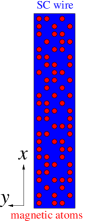
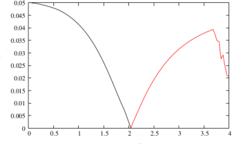
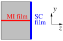
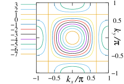
Device design: In the first device (see Fig. 1a), we use a layered SC wire to realize 1D TSC. The layered SC wire is formed by an -wave monolayer thin film or a layered -wave SC material. The width of the wire should be less than the superconducting coherent length (smaller is better). We also cover the wire with isolated magnetic atoms which can have a uniform or a random distribution (the more uniform the better). In this case, we find that, even for a weak MEC (about 1/4 of the Fermi energy or 1/16 of bandwidth), a spiral magnetic order of the magnetic atoms will develop automatically to produce an 1D TSC with a sizable gap (about 1/2 of the parent superconducting gap). If the magnetic atoms have a perfect uniform distribution (i.e. form a periodic lattice), the required MEC is even smaller (of order of the interlayer hopping amplitude or the gap of the parent superconductor), and the gap of the induced TSC is close to that of the parent superconductor (see Fig. 1b).
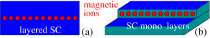
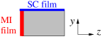
In the second device (see Fig. 2a), we use a layered superconductor (such as FeSe) or a mon-layer superconductor. We put a line of isolated magnetic atoms on the superconducing surface, where the separation of the magnetic atoms is less than the superconducting coherence length. We require the magnetic atom to be ionized and cause a local shift of chemical potential in the superconducting layer under the magnetic atoms. We find that if the shift of the chemical potential is of the order of the Fermi energy, then even for a weak MEC (much less than the bandwidth), a spiral magnetic order of the magnetic atoms will develop automatically to produce an 1D TSC with a large gap (close to the parent superconducting gap) (see Fig. 3b,c,d,f,g,h).


(a)
(b)
(c)
(d)


 (e)
(f)
(g)
(h)
(e)
(f)
(g)
(h)
In LABEL:NDL1446,PM150506078, a device formed by a mono-atomic chain of Fe atoms on the surface of superconducting Pb was fabricated. The Fe atoms touch each other and form a metallic wire as described in LABEL:KD14017048, assuming the Fe-chain is very long. For this first class of devices, a strong MEC is not required and a weak MEC is enough to induce a TSC. However, in the experiment, the Fe-chain is very short (less than the superconducting coherent length) and MZMs at the chain ends, if any, may not be isolated. In this paper, we consider the case where the magnetic atoms do not touch each other and form an insulating wire. We will use Yu-Shiba-Rusinov states induced by MEC to form the 1D TSC.
In LABEL:ZK171010701, quantized resonance conductance for a MZM was observed. The energy scale that protects the MZM is about K, which is much less than the energy scale for the parent superconductor K. In this paper, we try to design devices to produce the 1D TSC whose energy gap is close to that of the parent superconductor (see Fig. 1). For a quantum wire made by FeSe monolayer on SrTiO3, such a gap can be as large as meVK.
Model for the first device: Since the 1D SC wire is formed a monolayer film or a layered material, if we ignore the interlayer hopping, we can model such a wire covered magnetic atoms by a 2D model on a square lattice of size (see Fig. 1):
| (1) |
where , and sums over the sites with the magnetic atoms. describes the MEC to the magnetic atoms where the unit vectors describe the spin orientation of the magnetic atoms. describes potential shift caused by the magnetic atoms. We will choose , (i.e. ), , and where is the lattice constant. Such a system has a generic circular Fermi surface. The corresponding superconducting coherent length is . The above choice of parameters roughly models the FeSe monolayer.
We further assume the magnetic atoms to have a spiral magnetic order
| (2) |
where is spiral wave-vector. is a dynamical parameter. The ground state has a that minimizes the total energy.
Assuming one magnetic atom per site with (i.e. a uniform distribution), we find a phase diagram in Fig. 1b via a numerical calculation of the energy spectrum of eqn. ( Realizing Majorana zero mode with a stripe of ionized and isolated magnetic atoms on a layered superconductor). (The uniform case is also studied in LABEL:SB14101734.) The Yu-Shiba-Rusinov states Yu (1965); Shiba (1968); Rusinov (1969) induced by the MEC of magnetic atoms have a size of , whose centers have a separation . So the Yu-Shiba-Rusinov states strongly overlap with each other. Those overlapping Yu-Shiba-Rusinov states can form a TSC if the spins of the magnetic atoms form a proper spiral order. In Fig. 1b, we see that a spiral order with marked white is spontaneously generated to minimize the ground state energy (see Supplementary Materials Section I). For such a spiral order, the Yu-Shiba-Rusinov states automatically form the TSC with MZMs protected by a large energy gap. Even in the limit , we find the gap of the TSC can be close to the gap of parent superconductor. For example, for a weak MEC , the gap of TSC can reach .
The spiral order that minimizes the ground state energy usually produce a TSC. This is because the Yu-Shiba-Rusinov states correspond to spinless electrons. When 1D spinless electrons want to form a gapped superconducting state to minimize the ground state energy, the -wave superconductivity is the only option. We also like to remark that the number of “wedges” in the phase diagram for small is the number of 1D subbands, which is given by , where is the Fermi wave-vector. Thus the SC wire should be very narrow in order not to have too many subbands.
Our model actually has a twisted time reversal symmetry , generated by the usual time reversal and 180∘ spin- rotation (assuming the magnetic order is in -plane). The time reversal symmetry is described by symmetry group. The 1D fermionic topological phases with time reversal symmetry are classified by integersFidkowski and Kitaev (2010) – the number of the MZMs at one end of the wire (see Supplementary materials Section II). The odd- phases correspond to iTO, and the even- phases correspond to symmetry protected topological (SPT) orders.Gu and Wen (2009)
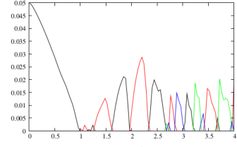
The TSC phase is also robust against disorder in the local density of the magnetic atoms. Fig. 1c is the phase diagram for , , , and there are 0.3 magnetic atoms per site. (The percolation threshold is 0.592 atoms per site.) Again, for the spiral order that minimizes the ground state energy, the Yu-Shiba-Rusinov states automatically form the TSC with MZMs. For a weak MEC , the gap of TSC is about . Fig. 1d is the phase diagram for even stronger potential shift .
We see that the randomness in the MEC and the chemical potential caused by the random distribution of the magnetic atom increase the required MEC and reduce the gap of TSC. But even with that randomness, the required MEC is still quite weak: (for ).
The system in Fig. 1 models a SC wire whose width is 10 lattice spacing (a few nanometers). The SC coherent length is also a few nanometers. (But a longer SC coherent length will not significantly affect our results, see Supplementary Materials Fig. 18:Right.) The wire is covered by magnetic atoms with a density of per site, which is well below the percolation threshold of 0.592 atoms per site. In fact, the above parameters fit a SC wire made by FeSe superconducting thin film quite well.
In the following, we summarize some key factors in the device design to realize the 1D TSC with MZMs:
-
1.
A SC wire is formed by a monolayer thin film, or quasi-2D material (such as FeSe superconductor with nm), or material whose Fermi surface contains tube-like parts or parallel sheets.
-
2.
The parent superconductor is an -wave superconductor with no spin-orbital coupling, or the spin-orbital coupling still conserves one component of the spin.
-
3.
The width of the SC wire is a few times , which is less than the SC coherent length . LABEL:LC10060420 has developed a method to make nano-wires as narrow as nm.
-
4.
The SC wire is covered by isolated magnetic atoms that do not touch each other. Note that the distribution of the magnetic atoms can be random, as long as their density is much higher than .
-
5.
The magnetic atoms have a weak spin-orbital coupling less than the superconducting gap , so that the spins can rotate freely.
-
6.
If the magnetic atoms have a random distribution, they should not cause a too large local chemical potential shift . If the magnetic atoms have a uniform distribution, then a large local chemical potential shift may help to produce the 1D TSC for weak MECs. In this case, we do not need a SC wire, since the magnetic atoms can make an effective SC wire by themselves.
The resulting device can realize TSC with a sizable gap ( of parent superconducting gap), even for a weak MEC ().
Model for the second device: However, it is hard to make a very narrow superconducting wire. To solve this problem, we propose a second device (see Fig. 2a). In this device, we place a line of isolated magnetic atoms on the surface of a layered superconductor, such as FeSe. But now we require the magnetic atoms to cause a large local chemical potential shift . In this case, the magnetic atoms will induce an effective SC wire under them, which may lead to a 1D TSC state. We still use eqn. ( Realizing Majorana zero mode with a stripe of ionized and isolated magnetic atoms on a layered superconductor) to model our device. We will assume , , and . We still assume the magnetic atoms to have a spiral magnetic order described by eqn. (2). The resulting phase diagram is given in Fig. 3a,b,c,d. (Note that, on the FeSe surface, magnetic atoms separated by one lattice spacing can still be isolated.)
From Fig. 3a, we find that if the magnetic atoms do not dope the superconductor (i.e. the local shift of the chemical potential ), then the TSC phase cannot be realized by the ground state of the spin spiral state, for weak MEC . From Fig. 3b,c,d, we find that if the magnetic atoms dope the superconductor (i.e. the local shift of the chemical potential ), then the ground state of the spin spiral state also realize the TSC phase for weak MEC . The induced 1D TSC state has a gap close to that of the parent SC state. We like to remark that if the FeSe layers have steps on the surface, placing the magnetic atoms along a straight step (see Fig. 2b) will help to produce the 1D TSC state.
In Fig. 3b, the local doping enlarge the electron-like Fermi surface. In Fig. 3c, the local doping creates an electron-like Fermi surface. In Fig. 3d, the local doping change the electron-like Fermi surface to a hole-like Fermi surface. In those three cases, we see that the local doping from the magnetic atoms can produce an effective SC wire on a surface of layered SC. The spin of the magnetic atoms will develop a spiral order to realize the TSC phase even for a weak MEC (about 1/5 of the Fermi energy 1/20 of the bandwidth). The gap of the STC is about that same as the parent SC gap.
In Fig. 3e,f,g,h, we also consider a device where the magnetic atoms form a line at a step edge of the SC thin film. Here we allow the electron to have a random distribution with each occupied by 1 or 0 atoms. The average density is atoms per site. In Fig. 3f, the local doping enlarge the electron-like Fermi surface. In Fig. 3g, the local doping creates an electron-like Fermi surface. In Fig. 3h, the local doping change the electron-like Fermi surface to a hole-like Fermi surface. In those three cases, the magnetic atoms can still realize the TSC phase for a weak MEC (about 1/5 of the Fermi energy 1/20 of the bandwidth). The gap of the STC can be as large as 1/2 of the parent SC gap. We would like to remark that if the SC thin film, such as FeSe layers have steps on the surface, placing the magnetic atoms along a straight step (see Fig. 2b) will help to produce the 1D TSC state, which will be even stronger than that shown in Fig. 3b,c,d.
We would like to thank A. Chang, J.-F. Jia, P.A. Lee, J.-W. Mei, J.S. Moodera, G. Wang, H.-H. Wen, and Q.-K. Xue for helpful discussions. This work is supported by NSF grant DMR-1506475 and DMS-1664412.
Supplementary Materials
I Ground state energy of a superconductor
In general, a superconductor is described by
| (3) |
where labels the electron spin and site position. In Majorana basis
| (4) | ||||
becomes
| (5) |
where
| (6) |
Note that satisfies
| (7) |
We can use an orthogonal matrix to transforms into the canonical form
| (8) |
Now becomes
| (9) |
Note that has eigenvalues and with different ’s commute with each other. The ground state satisfies
| (10) |
The groud state energy is given by
| (11) |
II The fermionic SPT phases protected by time reversal symmetry
In the presence of time-reversal symmetry, the hopping coefficient and are real, and we have
| (12) |
In this case
| (13) |
In the gapped phase . Thus wind number , the number of times wind around as we change to is well defined. Such a winding number characterizes the -SPT order of the gapped 1D SMI-SC junction. The -SPT state will have number of MZM’s at an end of the 1D SMI-SC junction.
III Some other device designs to produce MZMs
In this section, we consider some other device designs that can produce MZMs. We will consider junction between a stripe of spiral magnetic insulator (SMI) and an -wave superconductor. We find that, in general, that those devices can give rise to the 1D TSC phase only when the magnetic exchanging coupling is of order the bandwidth of the SC. In the following, we will concentrate on how to design devices that can realize the 1D TSC phase with a gap close to the SC gap at small magnetic exchanging couplings.
III.1 Two coupled ferromagnetic dots
First, we note that a magnetic atom at the surface of superconductor induces an energy level in the superconductor below the SC gap. The energy level has its spin pointing in direction. Two magnetic atoms will induce two energy levels inside the SC gap. Two nearby energy levels with spins and have the following form of coupling which contains both hopping and pairing terms:
| (14) |
The spin- wave function is given by
| (15) |
where . We find
| (16) | |||
When , the above becomes
| (17) |
We see that the strength of the hopping coupling and the -wave pairing coupling can be tuned by the angle between the two spins on the two dots. A uniform hopping coupling and -wave pairing coupling can be obtained with spiral magnetic order. This motivates us to consider a SC thin film coupled to a spiral magnetic order.
III.2 A SC sample coupled to a spiral magnetic insulator
Let us first consider the device in Fig. 4, which is described by the model eqn. (III.4). We introduce the following site-dependent spin- rotation
| (18) |
to change the Hamiltonian to
| (19) |
where
| (20) |
The model has a translation symmetry in -direction, and satisfies
| (21) |


After the Fourier transformation in -direction, we obtain
| (22) |
The band structure is determined by the matrix
| (23) |
where the matrices and can be obtained from (III.2).
In Majorana basis
| (24) |
becomes
| (25) | |||
where . The energy bands are given by the eigenvalues of . If the lowest band is non zero for all , then the 1D SMI-SC junction is gapped. Such a gapped state may be in a non-trivial TSC phase (with odd number of MZM at an end of the 1D SMI-SC junction), or in a trivial phase without MZM. We can detect the TSC phase by computing Pfaffian of at where are real anti-symmetric matrices. If , the gapped phase is the TSC phase. And if , the gapped phase is the trivial phase.
In fact in the presence of translation symmetry in -direction, there are actually four different phases, charactered by the signs of and . The phase with and is trivial, while the phase with and is non-trivial SPT phase protected by -translation symmetry.
III.3 Examples of SMI-SC heterostructures
In this section, we study various examples of SMI-SC junctions, and identify the conditions to realize the 1D TSC phase with weak MEC and a large gap.
III.3.1 A SC bulk sample coupled to a spiral magnetic stripe
First let us consider a bulk -wave superconductor on cubic lattice where in the model (III.4) are given by
| (26) |
(In this paper, we always choose the nearest neighbor hopping in -direction and the lattice constant .) We choose the chemical potential to be so that the superconductor has a typical spherical Fermi surface. The bulk superconductor is coupled to a spiral magnetic insulator stripe in -direction on its - surface (see Fig. 5). We take the superconducting gap to be and the spiral wave vector . The width of the spiral magnetic insulator stripe is and (the later is about the SC coherent length). We obtain a phase diagram (see Fig. 6) of the 1D SMI-SC junction, as we vary the MEC .
From Figs. 6, we see that the 1D TSC phase does appear. But the TSC phase only appears for very strong MEC . The superconducting gap is only . Naively, we would expect to obtain the 1D TSC phase when .


However, the magnetic insulator only interact with the first surface layer of SC sample. The energy shift of a spin polarized level caused by the MEC is given by
| (27) |
where is the lattice constant, is the size of the wave function of the spin polarized level in the direction perpendicular to the 1D SMI-SC junction, and the is the typical Fermi velocity in the direction perpendicular to the 1D SMI-SC junction. We see that MEC need to be to push a spin polarized levels down to near zero energy (i.e. ), so that those levels can organize into the TSC phase.
Thus, the key to realize the 1D TSC phase at weaker MECs is to reduce transverse velocity . This can be achieved if Fermi surface of the superconductor has flat parts, and the 1D SMI-SC junction is perpendicular to the flat parts.


III.3.2 A quasi 1D SC thin film coupled to a spiral magnet along its edge
One way to reduce is to simply use quasi 1D superconductors. Recently, some quasi 1D superconductors were discovered, such as Tl2-xMo6Se6 (K, ), K2Cr3As3 (K), Rh2Cr3As3 (K), Cs2Cr3As3 (K), RbCr3As3 (K), KCr3As3 (K).Bergk et al. (2011); Bao et al. (2015) Without doping, the Fermi wave vector along the 1D chain is with .
Let us assume that we can make a thin film of the quasi 1D superconductors, and we consider SMI-SC junction in Fig. 4, where the 1D chain is parallel to the junction. We choose the width of the magnetic stripe to be the same as the thickness of the SC thin film. We model the quasi 1D superconductors by reducing from 1 to , and obtain the phase diagram as in Fig. 7. We see that the required MEC is much reduced to the scale of the interchain coupling in the quasi 1D superconductor. Even for small MEC, the gap of the 1D TSC phase can be close to the superconducting gap . Increasing the thickness SC thin film from to does not reduce the 1D TSC gap by much.
However, the above-mentioned benefits come with a cost: the TSC phase can
appear at small MECs only for a window of chemical potentials (or a
window of the dopings of the SC film). This is because, in order for the TSC
phase to appear at small MECs, the following conditions need to be satisfied:
(1) the density of states per unit cell per unit and per
unit has peaks, and
(2) the spiral wave vector can
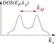
connect the peaks (see Fig. 8).
As we change , the
separation between the peaks can change, and we obtain TSC when the peak
separation matches .
To see the above condition more clearly, we introduce the following overlap of the resolved density of states :
| (28) |
We plotted for our model of quasi 1D superconductor in Fig. 9. The overlap-density of states becomes large () in a window which match the window of the chemical potentials, for the TSC phase to appear at small MECs (see Fig. 7).
This is a key result in this section: To realize TSC phase for small MECs, we need to find superconductor whose band structure gives rise to large , such as in unit as one can see from Fig. 9. For a typical superconductor with , the overlap-density of states is given by Fig. 10, where for all . At chemical potential , . This explains why we need a very large MEC to realize the topological SC phase.
The phase diagram Fig. 7 is for a very large spiral wave vector . Such a large spiral vector can appear in triangle-lattice magnetic materials, such as CuCrO2. We also see that the TSC phase does not appear for undoped quasi 1D superconductors with chemical potential and Fermi wavevector . To obtain TSC, we must dope the quasi 1D superconductors to shift chemical potential away from zero. The 10% doping of the quasi 1D superconductors has been achieved, which corresponds to . For such doping, the TSC phase does not appear for small MEC if the thickness of the SC thin film is . But for , the topological SC phase appear for and . However, it is highly non-trivial to find a match between quasi 1D superconductor and SMI so that they can form a good junction as in Fig. 4.
III.3.3 Superconductors with flat Fermi surfaces
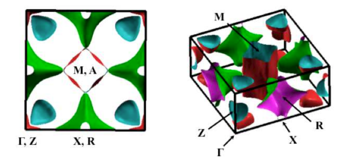


We have seen that a small transverse velocity is very helpful to obtain 1D TSC phase for small MECs. In addition to quasi 1D superconductors, another way to realize small transverse velocity is to use superconductor with flat Fermi surfaces, such as NbSe2 Borisenko et al. (2009) (see Fig. 15) and BaTi2A2O where A = As, Sb, Bi (see Fig. 16). In particular, NbSe2 has two advantages. First, it is a layered material, with two-dimensional character. It can even be made into a monolayer. Second, NbSe2 can be doped and its chemical potential can be tuned continuously.Xi et al. (2016)
We construct the device by putting magnetic atoms on the above superconductors. The magnetic atoms form a 1D array along the normal direction of the flat Fermi surface. It is important that the magnetic atoms do not touch each other, so that the magnetic atoms do not form a 1D metallic wire.
We can model such superconductors and their flat Fermi surfaces by choosing
| (29) |
(We only consider monolayer SC thin film by choosing .) When the Fermi energy is near , there are two pairs of parallel flat Fermi surfaces, which are separated by (see Fig. 12). Putting magnetic atoms with a spiral magnetic moment on such a SC, we obtain the phase diagram as in Fig. 14. We see that 1D TSC phase appears for very small MECs. If we put the array of magnetic atoms on the edge of the SC thin film, the maximum gap of the TSC is about . If we put the array of magnetic atoms in the middle of the SC thin film, the maximum gap of the TSC is about .
III.4 Engineer a superconducting wire
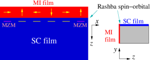
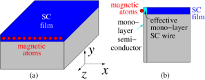
If the Fermi surface of SC material contains tube-like parts or parallel sheets (see Fig. 15 and Fig. 16), then the SC material is effectively a quasi-2D or a quasi-1D material for our purpose of making 1D TSC. In this case, we can use a SC thin film to mimic a quantum wire. Instead of putting isolated magnetic atoms on a quantum wire, we can put the isolated magnetic atoms on the side of the SC thin film (see Fig. 17a). The thickness of the SC film should be a few times . We expect that a spiral magnetic order on the magnetic atoms will develop spontaneously to produce a 1D -wave topological superconductor with MZM at ends of the chain.
For generic SC materials without tube-like Fermi surfaces or parallel Fermi surfaces, we need a very strong MEC to realize 1D TSC (see Supplementary Materials Fig. 18:Left). However, if the superconductor has well-localized surface states, those surface states on the edge of the SC film may couple strongly to the magnetic atoms. In this case, we may not need a strong MEC to realize 1D TSC and its MZM.
We may even engineer those surface states by evaporating a thin layer of certain atoms on the edge of the film. For example, we can evaporate a monolayer of semiconductor on the cleaved edge of the SC thin film. We hope the SC thin film to dope the semiconducting monolayer, and the semiconducting monolayer becomes superconducting due to the proximity effect. Note that the superconducting electrons in the semiconducting monolayer are well localized inside the monolayer. This way, we obtain an effective monolayer SC wire on the cleaved edge of the SC film, which is well modeled by eqn. ( Realizing Majorana zero mode with a stripe of ionized and isolated magnetic atoms on a layered superconductor). If we can find a superconducting/metallic atom that only sticks to the SC thin film, rather than the substrate, then we can evaporate a monolayer of such superconducting/metallic atoms to engineer an effective monolayer SC wire on the edge of the SC film (See Fig. 17b).
To confirm the validity of the above design, we consider the following model to describe the SC thin film
| (30) |
where ,
| (31) |
describes the MEC to the magnetic atoms. Here
| (32) |
i.e. the MEC only couples to the first layer (marked by ) on the SC surface. We choose , , , and . Such a SC film has an electron-like Fermi surface and a superconducting coherent length , We also assume one magnetic atom per site (i.e. no randomness), which gives us a phase diagram Fig. 18:Left. We see that only for MEC can the TSC phase appear.
We can model the monolayer of semiconductor by changing the chemical potential to at the SC surface layer (at ). We also set the proximity induced superconducting gap at the surface layer to be . If we choose , the surface monolayer will have a smaller electron-like Fermi surface. We obtain a phase diagram Fig. 18:Middle with TSC phase for . We see that adding a monolayer of “similar” atoms does not help.
If we choose , the surface monolayer will have a hole-like Fermi surface which is very different from the bulk SC film. We obtain a phase diagram Fig. 18:Right. We see that adding a monolayer of “very different” atoms makes the TSC appear at very weak MEC . For MEC , the gap of TSC is about .
Thus it is important that the monolayer is formed with atoms that have a very different band structure than the bulk SC film, such as one has electron-like Fermi surfaces and the other has hole-like Fermi surfaces. We see that the cleave-edge overgrowth of a monolayer of “very different” atoms on a SC thin film, plus a dilute layer of isolated magnetic atoms, is a practical way to realize MZM.
References
- Wen (1995) X.-G. Wen, Adv. Phys. 44, 405 (1995), cond-mat/9506066 .
- Kong and Wen (2014) L. Kong and X.-G. Wen, (2014), arXiv:1405.5858 .
- Freed (2014) D. S. Freed, (2014), arXiv:1406.7278 .
- von Klitzing et al. (1980) K. von Klitzing, G. Dorda, and M. Pepper, Phys. Rev. Lett. 45, 494 (1980).
- Johnson and McCoy (1971) J. D. Johnson and B. M. McCoy, Phys. Rev. A 4, 2314 (1971).
- Kitaev (2001) A. Y. Kitaev, Phys.-Usp. 44, 131 (2001), cond-mat/0010440 .
- Senthil et al. (1999) T. Senthil, J. B. Marston, and M. P. A. Fisher, Phys. Rev. B 60, 4245 (1999), cond-mat/9902062 .
- Read and Green (2000) N. Read and D. Green, Phys. Rev. B 61, 10267 (2000).
- Wen and Niu (1990) X. G. Wen and Q. Niu, Phys. Rev. B 41, 9377 (1990).
- Kitaev (2003) A. Y. Kitaev, Ann. Phys. (N.Y.) 303, 2 (2003).
- Wen (1991) X.-G. Wen, Phys. Rev. Lett. 66, 802 (1991).
- Moore and Read (1991) G. Moore and N. Read, Nucl. Phys. B 360, 362 (1991).
- Ivanov (2001) D. A. Ivanov, Phys. Rev. Lett. 86, 268 (2001), cond-mat/0005069 .
- Sau et al. (2010) J. D. Sau, R. M. Lutchyn, S. Tewari, and S. Das Sarma, Physical Review Letters 104, 040502 (2010), arXiv:0907.2239 .
- Oreg et al. (2010) Y. Oreg, G. Refael, and F. von Oppen, Physical Review Letters 105, 177002 (2010), arXiv:1003.1145 .
- Potter and Lee (2012) A. C. Potter and P. A. Lee, Phys. Rev. B 85, 094516 (2012), arXiv:1201.2176 .
- Klinovaja et al. (2012) J. Klinovaja, P. Stano, and D. Loss, Physical Review Letters 109, 236801 (2012), arXiv:1207.7322 .
- Kim et al. (2014) Y. Kim, M. Cheng, B. Bauer, R. M. Lutchyn, and S. Das Sarma, Phys. Rev. B 90, 060401 (2014), arXiv:1401.7048 .
- Choy et al. (2011) T.-P. Choy, J. M. Edge, A. R. Akhmerov, and C. W. J. Beenakker, Phys. Rev. B 84, 195442 (2011), arXiv:1108.0419 .
- Nadj-Perge et al. (2013) S. Nadj-Perge, I. K. Drozdov, B. A. Bernevig, and A. Yazdani, Phys. Rev. B 88, 020407 (2013), arXiv:1303.6363 .
- Klinovaja et al. (2013) J. Klinovaja, P. Stano, A. Yazdani, and D. Loss, Physical Review Letters 111, 186805 (2013), arXiv:1307.1442 .
- Braunecker and Simon (2013) B. Braunecker and P. Simon, Physical Review Letters 111, 147202 (2013), arXiv:1307.2431 .
- Vazifeh and Franz (2013) M. M. Vazifeh and M. Franz, Physical Review Letters 111, 206802 (2013), arXiv:1307.2279 .
- Reis et al. (2014) I. Reis, D. J. J. Marchand, and M. Franz, Phys. Rev. B 90, 085124 (2014), arXiv:1406.5222 .
- Dumitrescu et al. (2014) E. Dumitrescu, B. Roberts, S. Tewari, J. D. Sau, and S. Das Sarma, (2014), arXiv:1410.5412 .
- Schecter et al. (2016) M. Schecter, K. Flensberg, M. H. Christensen, B. M. Andersen, and J. Paaske, Phys. Rev. B 93, 140503 (2016), arXiv:1509.07399 .
- Xiao and An (2015) J. Xiao and J. An, New Journal of Physics 17, 113034 (2015), arXiv:1510.08308 .
- Christensen et al. (2016) M. H. Christensen, M. Schecter, K. Flensberg, B. M. Andersen, and J. Paaske, Phys. Rev. B 94, 144509 (2016), arXiv:1607.08190 .
- Yu (1965) L. Yu, Acta Phys. Sin. 21, 75 (1965).
- Shiba (1968) H. Shiba, Progress of Theoretical Physics 40, 435 (1968).
- Rusinov (1969) A. I. Rusinov, JETP Lett 9, 85 (1969).
- Nadj-Perge et al. (2014) S. Nadj-Perge, I. K. Drozdov, J. Li, H. Chen, S. Jeon, J. Seo, A. H. MacDonald, B. A. Bernevig, and A. Yazdani, Science 346, 602 (2014).
- Pawlak et al. (2016) R. Pawlak, M. Kisiel, J. Klinovaja, T. Meier, S. Kawai, T. Glatzel, D. Loss, and E. Meyer, npj Quantum Information 2, 16035 (2016), arXiv:1505.06078 .
- Zhang et al. (2018) H. Zhang, C.-X. Liu, S. Gazibegovic, D. Xu, J. A. Logan, G. Wang, N. van Loo, J. D. S. Bommer, M. W. A. de Moor, D. Car, R. L. M. Op Het Veld, P. J. van Veldhoven, S. Koelling, M. A. Verheijen, M. Pendharkar, D. J. Pennachio, B. Shojaei, J. S. Lee, C. J. Palmstrøm, E. P. A. M. Bakkers, S. D. Sarma, and L. P. Kouwenhoven, Nature 556, 74 (2018), arXiv:1710.10701 .
- Sedlmayr et al. (2015) N. Sedlmayr, J. M. Aguiar-Hualde, and C. Bena, Phys. Rev. B 91, 115415 (2015), arXiv:1410.1734 .
- Fidkowski and Kitaev (2010) L. Fidkowski and A. Kitaev, Phys. Rev. B 81, 134509 (2010), arXiv:0904.2197 .
- Gu and Wen (2009) Z.-C. Gu and X.-G. Wen, Phys. Rev. B 80, 155131 (2009), arXiv:0903.1069 .
- Li et al. (2011) P. Li, P. M. Wu, Y. Bomze, I. V. Borzenets, G. Finkelstein, and A. M. Chang, Phys. Rev. Lett. 107, 137004 (2011), arXiv:1006.0420 .
- Bergk et al. (2011) B. Bergk, A. P. Petrović, Z. Wang, Y. Wang, D. Salloum, P. Gougeon, M. Potel, and R. Lortz, New Journal of Physics 13, 103018 (2011), arXiv:1106.2405 .
- Bao et al. (2015) J.-K. Bao, J.-Y. Liu, C.-W. Ma, Z.-H. Meng, Z.-T. Tang, Y.-L. Sun, H.-F. Zhai, H. Jiang, H. Bai, C.-M. Feng, Z.-A. Xu, and G.-H. Cao, Physical Review X 5, 011013 (2015), arXiv:1412.0067 .
- Borisenko et al. (2009) S. V. Borisenko, A. A. Kordyuk, V. B. Zabolotnyy, D. S. Inosov, D. Evtushinsky, B. Büchner, A. N. Yaresko, A. Varykhalov, R. Follath, W. Eberhardt, L. Patthey, and H. Berger, Phys. Rev. Lett. 102, 166402 (2009).
- Xi et al. (2016) X. Xi, H. Berger, L. Forró, J. Shan, and K. F. Mak, Physical review letters 117, 106801 (2016).
- Nakano et al. (2016) K. Nakano, K. Hongo, and R. Maezono, Scientific Reports 6, 29661 (2016), arXiv:1602.02024 .