Magnetism and Magneto-optical Effects in Bulk and Few-layer CrI3: A Theoretical GGA + U Study
Abstract
The latest discovery of ferromagnetism in atomically thin films of semiconductors Cr2Ge2Te6 and CrI3 has unleashed numerous opportunities for fundamental physics of magnetism in two-dimensional (2D) limit and also for technological applications based on 2D magnetic materials. To exploit these 2D magnetic materials, however, the mechanisms that control their physical properties should be thoroughly understood. In this paper, we present a comprehensive theoretical study of the magnetic, electronic, optical and magneto-optical properties of multilayers [monolayer (ML), bilayer and trilayer] as well as bulk CrI3, based on the density functional theory with the generalized gradient approximation plus on-site Coulomb repulsion scheme. Interestingly, all the structures are found to be single-spin ferromagnetic semiconductors. They all have a large out-of-plane magnetic anisotropy energy (MAE) of 0.5 meV/Cr, in contrast to the significantly thickness-dependent MAE in multilayers of Cr2Ge2Te6. These large MAEs suppress transverse spin fluctuations and thus stabilize long-range magnetic orders at finite temperatures down to the ML limit. They also exhibit strong magneto-optical (MO) effects with their Kerr and Faraday rotation angles being comparable to that of best-known bulk MO materials. The shape and position of the main features in the optical and MO spectra are found to be nearly thickness-independent although the magnitude of Ker rotation angles increases monotonically with the film thickness. Magnetic transition temperatures estimated based on calculated exchange coupling parameters, calculated optical conductivity spectra, MO Kerr and Faraday rotation angles agree quite well with available experimental data. The calculated MAE as well as optical and magneto-optical properties are analyzed in terms of the calculated orbital-decomposed densities of states, band state symmetries and dipole selection rules. Our findings of large out-of-plane MAEs and strong MO effects in these single-spin ferromagnetic semiconducting CrI3 ultrathin films suggest that they will find valuable applications in semiconductor MO and spintronic nanodevices.
1 Introduction
The recent discovery of intrinsic ferromagnetism in atomically thin films of semiconductors Cr2Ge2Te6 [1] and CrI3 [2] has opened numerous exciting opportunities in two-dimensional (2D) magnetism. Amalgamation of magnetism and 2D materials are highly desirable for at least two reasons, one for exploration of fundamental physics of magnetism in 2D limit and the other for fascinating technological applications ranging from magnetic memories, to sensing, to spintronics to magneto-optical devices based on 2D materials. Therefore, these atomically thin magnetic materials are currently subject to intensive investigations. In fact, bulk CrI3 has already been well studied experimentally in the past [3, 4, 5] mainly because it is a layered ferromagnetic semiconductor with large Kerr and Faraday rotations which promise such device applications as optical insulators, magnetic sensors and rewritable optical memories [6]. Its 2D magnetic structures are presently attracting much renewed interest. For example, Seyler et al. [7] recently reported their observation of magneto-photoluminescence in monolayer and bilayer CrI3. Excitingly, manipulation of 2D magnetism (e.g., switching of magnetization direction and tuning antiferromagnetic to ferromagnetic transition) in BL CrI3 by either applying a vertical electric field [8, 9] or electrostatic doping [10] has also been recently demonstrated. Further, giant tunneling magnetoresistance has been observed in magnetic tunnel junctions made of atomically thin CrI3 and othe van der Waals (vdW) materials. [11, 12] Unprecedented control of spin and valley pseudospin in ultrathin CrI3 and WSe2 hetrostructures has also been demonstrated [13].
In order to exploit these emergent phenomena for various applications, the mechanisms that control the physical properties of these 2D materials should be thoroughly understood. As a step towards this goal, we present in this paper a comprehensive first-principles density functional study of the magnetic, electronic, optical and magneto-optical properties of multilayers [monolayer (ML), bilayer (BL) and trilayer (TL)] as well as bulk CrI3. Specifically, we focus the magnetic interactions, magnetic anisotropy energy and magneto-optical effects in these magnetic structures. Although magnetic exchange coupling and magnetic anisotropy in ML CrI3 have been theoretically investigated by several groups based on density functional calculations [14, 15, 16, 17], they have not been studied in BL, TL and bulk CrI3. Furthermore, the interlayer exchange coupling in bulk and TL CrI3 has not been addressed although that in the BL is presently under intensive investigations [18, 19, 20, 21].
Magnetic anisotropy energy (MAE) refers to the energy required to flip the magnetization from the easy to the hard axis, and is one of the principal specification parameters for a magnetic material. In fact, MAE is particularly important for 2D magnetic materials. According to the Mermin-Wagner theorem [22], a long-range magnetic order could not occur at any finite temperature in a 2D isotropic Heisenberg magnetic structure because of large thermal spin fluctuations in the 2D system. However, this Mermin-Wangner restriction [22] can be lifted if the 2D system has a significant out-of-plane MAE which would suppress the thermal fluctuations and thus stabilize the long-range magnetic order at finite temperature even in the ML limit, as was observed recently in ML CrI3 [2]. The MAE of a magnetic solid arises from two contributions, namely, the magnetocrystalline anisotropy energy (MCE) () due to the effect of electron relativistic spin-orbit coupling (SOC) on the band structure, and the magnetic dipolar anisotropy energy (MDE) () due to the magnetostatic dipole-dipole interaction in the magnetic solid. In a layered material, the MDE always prefers an in-plane magnetization while the MCE could favor either an in-plane or the out-of-plane magnetization depending on the band structure of the material. Although the MCE of ML CrI3 has been calculated [14, 17, 23], the MDE was not considered in these previous reports. Although the MDE is negligibly small for the cubic and isotropic materials such as bcc Fe and fcc Ni, it could become significant in low-dimensional materials [25, 24, 26]. In fact, it was found recently that although the MCE in ML Cr2Ge2Te6 favors the out-of-plane magnetization, the MDE is larger than the MCE such that ML Cr2Ge2Te6 would have an in-plane magnetization [26], thereby explaining why the longe-range ferromagnetic order was not observed in the ML [1]. Furthermore, there are no reports on the MAE of bulk, BL and TL CrI3. Therefore, in this paper we present both calculated MCE and MDE for all the considered CrI3 structures.
Magneto-optical (MO) effects are prominent manifestations of light-matter interactions in magnetic materials. When a linearly polarized light beam hits a magnetic material, the reflected and transmitted light beams would become elliptically polarized with the principal axis rotated with respect to the polarization direction of the incident light beam, as illustrated in Fig. 1(a). The former and latter are called MO Kerr (MOKE) and MO Faraday (MOFE) effects [27], respectively. MOKE has been widely used to probe the magnetic and electronic properties of solids, surface and thin films [27]. Indeed, long-range ferromagnetic orders in atomically thin films of Cr2Ge2Te6 and CrI3 were discovered by using the MOKE technique. [1, 2] In contrast, MOFE has been less explored mainly because light can only transmit through very thin films. Magnetic materials with large Kerr and Faraday rotations are the promising candidates for valuable magneto-optical device applications [28, 29], and thus they have continuously attracted attention in the past several decades. The latest discovery of 2D ferromagnetic semiconductors [1, 2] provides especially exciting possibilities of scaling the optical and magneto-optical devices down to subnanometer scale. Therefore, here we carry out a systematic first-principles density functional study of the optical and MO properties of bulk and multilayer CrI3. Indeed, our study reveals that bulk and multilayer CrI3 exhibit large MO effects in a wide optical frequency range with Kerr rotation angles being as large as 2.3 and Faraday rotation angles being in the order of 200°/m. This suggests that 2D ferromagnetic CrI3 semiconductor structures will provide an interesting material platform for further studies of novel magneto-optical phenomena and technological applications.
2 Computational methods
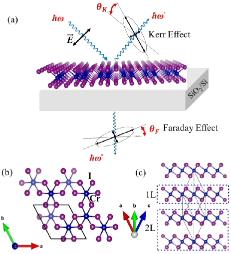
In this paper, we study the electronic, magnetic, and magneto-optical properties of bulk and multilayer CrI3 structures. Bulk CrI3 forms a layered structure with MLs separated by the van der Waals gap [Fig. 1(c)]. Each CrI3 ML consists of edge-sharing CrI6 octahedra forming a planar network with Cr atoms in a honeycomb lattice [Figs 1(b)] and thus there are two formula units (f.u.) per lateral unit cell. These MLs are then stacked in an ABC sequence, thus resulting in a rhombohedral crystal with symmetry and two f.u. per unit cell. This structure can also be regarded as an ABC-stacked hexagonal crystal with experimental lattice constants Å and Å [30]. We consider the experimental rhombohedral primitive cell in the bulk calculations. For the multilayer CrI3 structures, the hexagonal unit cell [Figs 1(b)] with the experimental lattice constants is considered as the lateral unit cell. For BL and TL CrI3 structures [see Fig. 1(c)], we consider the AB and ABC stackings, respectively. The slab-superlattice approach is used to construct the multilayer structures with the separations of neighboring slabs being at least 20 Å.
First-principles density functional calculations are performed using the accurate projector augmented wave (PAW) method [31] as implemented in the Vienna ab-initio simulation package (VASP) [32, 33]. The fully relativistic PAW potentials are adopted in order to include the SOC. The valence configurations of Cr and I atoms adopted in the calculations are 3d5 4s1, 5s2 5p5, respectively. A large plane-wave energy cutoff of 400 eV is used throughout the calculations. For the Brillouin zone integrations, -point meshes of 161616 and 20201 are used for bulk and multilayers CrI3, respectively.
The generalized gradient approximation (GGA) to the exchange-correlation potential of Perdew-Burke-Ernzerhof parametrization [34] is used. However, an improved account of onsite electron correlation among electrons is needed for a better description of the electronic and magnetic structures of transition metal compounds (see, e.g., Ref. [35] and references therein). To better describe onsite Coulomb repulsion between Cr electrons, we adopt the GGA+ scheme [36] in the present calculations. Feng et al. [26] recently carried out systematic GGA calculations for bulk and multilayer Cr2Ge2Te6 with different effective Coulomb energy values and concluded that the appropriate value for Cr electrons is 1.0 eV. Given the similarity between the Cr2Ge2Te6 and CrI3, here we also use eV. Nevertheless, we also perform a series of the GGA calculations with the value ranging from 0 to 3 eV for all the considered CrI3 systems and find that the calculated physical quantities do not depend significantly on the value used [see Supplementary Note A, table S1 and Fig. S1 in the Supplementary Information (SI)]. This indicates that the results presented below would remain nearly the same even if a different value were used.
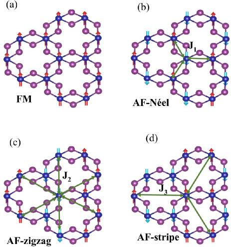
We consider four intra-layer magnetic configurations, namely, one FM as well as three antiferromagnetic (AF) structures, labelled as AF-Nel, AF-zigzag, and AF-stripe in Fig. 2. For bulk, BL and TL CrI3, we also consider interlayer FM and AF magnetic configurations with intralayer FM CrI3 MLs. To understand the magnetic interactions and also to estimate magnetic ordering temperature (Tc) for bulk and multilayers CrI3, we calculate the exchange coupling parameters by mapping the calculated total energies of these magnetic configurations (see Fig. 2) onto the classical Heisenberg Hamiltonian, where donates the nonmagnetic ground state energy; the exchange coupling parameter between sites and ; , the unit vector representing the direction of the magnetic moment on site . For one CrI3, we obtain a set of four linear equations of , and : and , which can be solved to estimate , and . Similarly, one can estimate the effective interlayer coupling parameter based the calculated total energies per unit cell of two magnetic configurations by using expressions for the BL, for the TL and for the bulk where denotes the total energy of the ferrimagnetic configuration with the Cr magnetic moments on one of the three layers in the hexagonal unit cell fliped.
We also calculate the MCE, MDE and hence MAE for all the considered structures in the FM state. We first perform two relativistic electronic structure calculations for the in-plane and out-of-plane magnetizations, and then obtain the MCE () as the total energy difference between the two calculations. Highly dense k-point meshes of 242424 and 28281 are used for bulk and multilayers CrI3, respectively. Further calculations by using different k-point meshes show that thus-obtained MCEs converge within 1 %. For a FM system, the MDE in atomic Rydberg units is given by [25, 24]
| (1) |
where the speed of light and the so-called magnetic dipolar Madelung constant
| (2) |
where R are the lattice vectors, q are the atomic position vectors in the unit cell, and is the atomic magnetic moment (in units of ) on site q. Using the calculated magnetic moments, the is obtained as the difference in between the in-plane and out-of-plane magnetizations. In a 2D material, since all the R and q are in-plane, the second term in Eq. (2) would be zero for the out-of-plane magnetization, thereby resulting in the positive while for an in-plane magnetization the is negative. [26] Therefore, the MDE always prefers an in-plane magnetization in a 2D material. This is purely a geometric effect and consequently the MDE is also known as the magnetic shape anisotropy energy.
In a FM solid with trigonal symmetry and magnetization rotational along -axis, the optical conductivity tensor consists of three independent elements, namely, , and . Within the Kubo linear response theory [37, 38], the adsorptive parts of these elements are given by
| (3) |
| (4) |
where is the photon energy, and is the th band energy at point . Summations and are over the occupied and unoccupied bands, respectively. Dipole matrix elements where denotes Cartesian component of the dipole operator, are obtained from the band structures within the PAW formalism [39], as implemented in the VASP package. The integration over the Brillouin zone is carried out by using the linear tetrahedron method (see Ref. [40] and references therein). The dispersive parts of the optical conductivity elements can be obtained using the Kramers-Kroing relations
| (5) |
| (6) |
where donates the principle value. The quasiparticle lifetime effects are accounted for by convoluting all the optical conductivity spectra with a Lorentzian of line width . For layered van der Waals materials such as graphite, is about 0.2 eV (see, e.g., Figs. 1(a) and 1(b) in Ref. [41]), which is thus used in this paper.
For a bulk magnetic material, the complex polar Kerr rotation angle is given by [42, 43],
| (7) |
However, for a magnetic thin film on a nonmagnetic substrate, the complex polar Kerr rotation angle is given by [44, 45]
| (8) |
where stands for the thickness of the magnetic layer and the diagonal part of the dielectric constant (optical conductivity) of the substrate. Experimentally, atomically thin CrI3 films were prepared on SiO2/Si [2, 13, 7]. Thus, the dielectric constant () of bulk SiO2 is used here.
Similarly, the complex Faraday rotation angle for a thin film can be written as [46]
| (9) |
where and represent the refractive indices for left- and right-handed polarized lights, respectively, and are related to the optical conductivity (or dielectric function) via expressions . Here the real parts of the optical conductivity can be written as
| (10) |
where . Clearly, , and thus would be nonzero only if and are different. In other words, magnetic circular dichroism is essential for the nonzero and hence the magneto-optical effects.
3 Results and discussion
3.1 Magnetic properties
3.1.1 Magnetic structure and exchange coupling:
To find the ground state magnetic structure and also evaluate exchange coupling among the magnetic Cr atoms in all the considered CrI3 structures, we first consider four possible intra-layer magnetic configurations, namely, the FM, Nel-type antiferromagnetic (AF-Nel), zigzag-antiferromagnetic (AF-zigzag) and stripe-like antiferromagnetic (AF-stripe) structures (see Fig. 2). The calculated total energies for these magnetic configurations indicate that for all the considered structures, the FM state is the most stable configuration. We then consider the interlayer ferromagnetic and antiferromagnetic [see Fig. 2(e)] structures for bulk, BL and TL CrI3, and again we find the interlayer FM state is more stable. Therefore, we list the calculated spin and orbital magnetic moments of bulk and multilayer CrI3 in the FM state only in Table 1. The calculated Cr spin magnetic moment in all the CrI3 structures is 3.2 , being in good agreement with the experimental value of 3.0 [30]. This is also consistent with three unpaired electrons in the Cr configuration in these structures. Further, the calculated Cr orbital magnetic moment for all the investigated structures is small ( 0.08 ), thus lending support to the notion of the completely filled spin-up Cr subshell in these systems. Interestingly, there is also a small induced magnetic moment (-0.09 ) on the I atom (Table 1), which is antipallel to that of the Cr magnetic moment, in all the systems. All these result in a total magnetic moment of 3.00 /f.u. for all the structures.
| () | () | () | () | () | ||
|---|---|---|---|---|---|---|
| (/f.u.) | (/atom) | (/atom) | (meV/f.u.) | (meV/f.u.) | (eV) | |
| ML | 6.00 | 3.20 (0.083) | -0.092 (-0.014) | 0.678 (-0.152) | 0.526 | 0.81 |
| BL | 6.00 | 3.21 (0.083) | -0.094 (-0.014) | 0.620 (-0.152) | 0.468 | 0.71 |
| TL | 6.00 | 3.21 (0.083) | -0.093 (-0.014) | 0.586 (-0.152) | 0.434 | 0.68 |
| Bulk | 6.00 | 3.21 (0.082) | -0.094 (-0.014) | 0.545 (-0.064) | 0.481 (0.26a) | 0.62 (1.2a) |
aRef. [3].
As mentioned in Sec. 2, using the total energies of the considered magnetic configurations, we estimate first three near-neighbor exchange coupling parameters (, , ) in each ML in all the considred systems and also the effective interlayer exchange coupling constant (). The calculated exchange coupling constants are listed in Table 2. It is clear from Table 2 that the first near-neighbor exchange coupling () is ferromagnetic (i.e., positive) in all the considered CrI3 structures. The second near-neighbor coupling () is also ferromagnetic (positive), although the value is about 3.5 times smaller than for all the structures. Interestingly, Table 2 shows that the magnitudes of both and increase monotonically with the number of layers, being consistent with the observed increase in magnetic transition temperature in these systemsi[2]. The third near-neighbor magnetic coupling () is also ferromagnetic (positive) in all the CrI3 structures except ML CrI3 where is negative (antiferromagnetic). Nonetheless, the calculated values are found to be 5 times smaller than and only about half of for all the structures. For the CrI3 ML, we find that all the calculated exchange coupling parameters are in good quantitive agreement with the recent GGA calculations [14, 15, 16], although the is slightly larger than that of the previous GGA+ calculation[17] with eV and eV. Note that only the first near-neighbor magnetic interaction was considered in Ref. [17] and also that the values reported previously [14, 15, 16, 17] should be multiplied by a factor of in order to compare with the present values.
Finally, we notice that the calculated interlayer exchange coupling constant is also ferromagnetic for bulk, BL and TL structures. This prediction agrees well with all previous experiments [2, 3, 4, 5] on all the structures except BL CrI3 which has been experimentally found to be interlayer antiferromagnetically coupled [2]. A microscopic explanation of this notable discrepancy between theory and experiment on BL CrI3 is nontrivial. Indeed, very recently this problem has already been investigated theoretically by several groups [18, 19, 20, 21]. These theoretical studies all showed that the interlayer magnetic coupling in BL CrI3 is strongly stacking dependent and is also sensitive to the exchange-correlation functional used. In particular, the GGA + calculation with eV [18] indicates that in the AB′-stacked BL CrI3, the total energy of the AF configuration is slightly lower than that of the FM configuration (by merely 0.7 meV/unit cell). However, the AB-stacking order which is the global minimum and favors the FM state, still have a total energy significantly lower than the AB′-stacked structure (by 6 meV/unit cell). Consequently, it was proposed [18] that BL CrI3 exfoliated at room-temperature is perhaps kinetically trapped in the metastable AB′-stacked structure, on cooling and thus the AF state was observed instead [2]. Furthermore, it was also found that even in the AB′-stacking order, the AF interlayer coupling becomes favorable only when is larger than 2.5 eV, [19] and this result is confirmed by our own GGA + calculations. Clearly, further measurements on the stacking order in BL CrI3 are needed to resolve this interesting problem. To this end, we calculate the optical and magneto-optical properties of BL CrI3 in both AB- and AB′-stacking orders. Unfortunately, we find that the magneto-optical effects of BL CrI3 hardly depend on the stacking order, as presented in Figs. S4 and S5 in the supplementary information.
3.1.2 Magnetic anisotropy energy and ferromagnetic transition temperature:
The calculated magnetic anisotropy energies () for bulk and multilayers CrI3 are presented in Table 1. As mentioned before, the MAE consists of two competing contributions, namely, magnetocrystalline anisotropy energy () due to the SOC effect on the band structure and magnetic dipolar (shape) anisotropy energy (). First of all, Table 1 shows that as could be expected from the 2D nature of their structures, the MDE per ML in all the considered systems is rather large and independent of the film thickness. Furthermore, the MDE is always negative and thus always prefers an in-plane magnetization. Remarkably, the MCE per ML is a few times larger than the MDE, and positive, meaning that it prefers the out-of-plane magnetization. The sum of these competing terms () thus results in the large and positive MAE (Table 1), which is more or less independent of the film thickness. This is in strong contrast to the case of the Cr2Ge2Te6 multilayers where the MAE is much smaller and depends significantly on the film thickness [26]. In particular, for ML Cr2Ge2Te6, the magnitude of MCE becomes smaller than that of MDE such that the MAE is negative, favoring an in-plane magnetization [26]. Importantly, since the significant out-of-plane MAE is needed to stabilize long-range magnetic orders in a 2D material by suppressing the thermal spin fluctuations, this explains why the FM state is observed in ML CrI3 [2] but not in ML Cr2Ge2Te6 [1]. These contrasting magnetic anisotropic properties between multilayers CrI3 and Cr2Ge2Te6 thus lend support to the notion that the former is well described by the 2D Ising model while the latter is well described by the Heisenberg model.[47]. Note that the present MCE of ML CrI3 is in good quantitative agreement with the theoretical value of 0.686 meV/f.u. reported recently in Ref. [14] in which the MDE was not calculated. Also, the calculated MAE of bulk CrI3 agree reasonably well with the experimental value reported in Ref. [3] (see Table 1). Since the MAEs of the CrI3 multilayers are large and comparable to heavy element magnetic alloys such as FePt and CoPt [48], which have the largest MAEs among magnetic transition metal alloys and compounds, these CrI3 multilayers could have valuable applications in high density data storage devices.
Now we consider the ferromagnetic transition temperature () of the CrI3 systems, which is another important parameter for a magnetic material. A rough estimation of could be made within the mean-field approximation (MFA), i.e., where and the present cases . [49] The estimated ferromagnetic transition temperatures () are listed in Table 2. It is clear from Table 2 that the estimated and measured agree in trend, i.e., the magnetic transition temperature increases monotonically from ML, to BL, to TL and to bulk CrI3. Nonetheless, the estimated values are much higher. In particular, for ML CrI3, the estimated of 109 K is more than two times larger than the experimental 45 K for ML CrI3, and in bulk CrI3, the of 191 K is about three times larger than the measured 61 K.[2]. The reason for this is that the MFA neglects transverse spin fluctuations [50, 51], which is especially strong in low-dimensional materials. Furthermore, the MFA violates Mermin-Wagner theorem [22] which says that long-range magnetic order at a finite temperature cannot exist in an isotropic 2D Heisenberg magnet. However, the out-of-plane MAE in 2D materials can establish long-range magnetic orders at finite temperatures by opening a gap in the spin wave spectrum which would suppress thermal spin fluctuations [50, 51]. Therefore, a better estimation of the would be based on the spin wave theory (SWT) with the out-of-plane MAE taken into account. This leads to an approximate expression of as where is the spin wave gap [17], which can be roughly set to . The values evaluated using the calculated and are listed in Table 2. It can be seen that compared with , the values agree better with the corresponding experimental values although they are still too high (Table 2).
3.2 Electronic structure
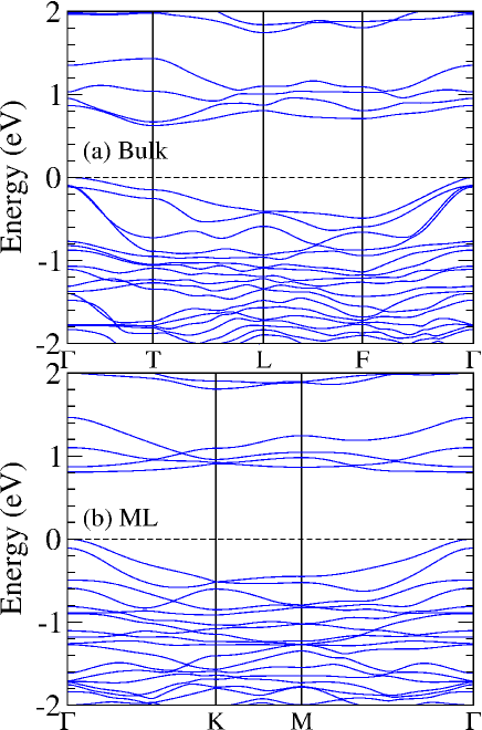
Better understanding of the electronic, magnetic and magneto-optical properties of the materials can be obtained from the detailed analysis of the electronic band structure. Therefore, fully relativistic electronic band structure of bulk and ML CrI3 structures are displayed in Fig. 3, while that of the BL and TL are displayed in Fig. S2 in the supplementary information (SI). Notably, these figures show that all the multilayer structures are almost direct band-gap semiconductors with both valance band maximum (VBM) and conduction band minimum (CBM) located at point. In contrast, the bulk structure is an indirect bandgap semiconductor with the VBM sitting at the point and the CBM located at the T point. The obtained semiconducting band gaps for all the structures are listed in Table 1, which shows that the band gap increases slightly as bulk CrI3 is thinned down to TL, to BL and finally to ML.
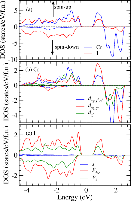
To analyze the spin characters of the bands at the VBM and CBM, we present the spin-polarized scalar-relativistic band structures of all the structures considered here in Fig. S3 in the SI. Figure S3 indicates that both the lower conduction bands and top valence bands of all the structures are of purely spin-up character. Interestingly, this shows that all the structures are single-spin semiconductors and thus would be promising candidates for efficient spintronic and spin photovoltaic devices (see Ref. [52] and references therein). We also calculate the total as well as site, orbital projected spin-up and spin-down densities of states (DOS) for all the CrI3 structures. The calculated DOS spectra of bulk and monolayer CrI3 are displayed in Figs. 4 and 5, respectively, as representatives. Figure 4 shows that the contributions to the valance and conduction bands in the energy ranges of -4.5 to -0.3 eV and 0.4 eV to 2.5 eV, respectively, come mostly from the Cr orbitals with significant contributions from the I orbitals as well. The contributions from both the Cr and I confirm the strong hybridization between Cr and I orbitals in CrI3 structures. The spin-up valance band states are predominately arise from the Cr orbitals, along with minor contribution with the I orbitals at the valence band edge. Conversely, the DOS states in spin-down valance band region are mostly contributed from I orbitals. The states in the upper valance band region of -4.5 eV to -0.3 eV are made up of spin-up Cr orbitals, with a broad peak at 1.3 eV. In case of conduction bands ranging from 0.4 eV to 1.2 eV is mainly because of spin-up Cr orbitals. From these one could say that the band gap in the CrI3 structures arise due to the crystal-field splitting of spin-up Cr and bands. The spin-down conduction bands appear only above 1.3 eV with pronounced peaks made up of mainly Cr and orbitals (Fig. 4). Furthermore, the calculated total as well as site, orbital projected spin-up and spin-down DOS spectra of ML CrI3 (Fig. 5) are rather similar to that of bulk CrI3 (Fig. 4). The main difference comes from the contributions of the I orbital which is enhanced in the higher energy region in the ML.
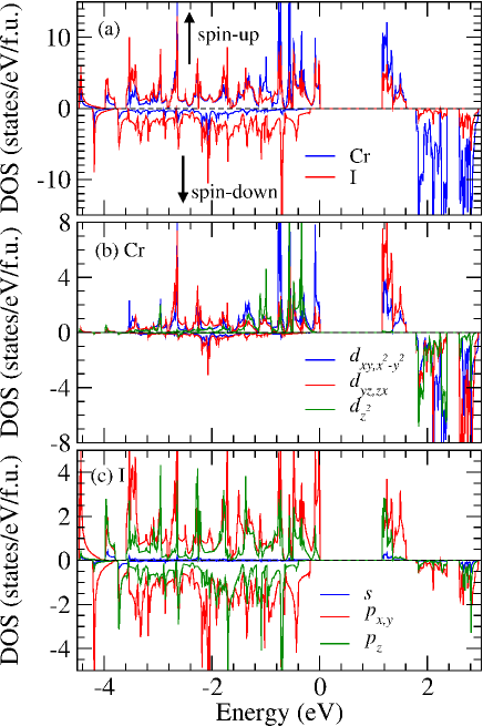
As mentioned above, the insulating band gap in the CrI3 structures arises due to the crystal-field splitting of Cr and states. The symmetries of these states near the band gap edges are important to the magneto-crystalline anisotropy in the presence of SOC [24, 53], according to the perturbation theory. In particular, the SOC matrix elements for the orbital of and would favor the perpendicular magnetic anisotropy, while other elements of , and would prefer an in-plane magnetic anisotropy [54]. The magnitude ratio of these -orbital SOC matrix elements are : : : : = [54]. Figures 4 and 5 show that in the upper valence and lower conduction band region, the and orbital-decomposed DOSs are large and this would result in large and and hence large contributions to the perpendicular anisotropy. In contrast, the DOS is almost zero in the lower conduction band region of 0.41.5 eV in both bulk and ML CrI3, and thus this would give rise to the diminishing SOC matrix element of which favors an in-plane magnetization. All these together would lead to the magneto-crystalline anisotropy energes in the CrI3 structures (see Table 1) which strongly favor the out-of-plane magnetization.
3.3 Optical conductivity
Now let us turn our attention to the calculated optical conductivity, which is the ingredient for evaluating the magneto-optical effects, as explained already in Sec. 2. The calculated optical conductivities of the investigated structures are displayed in Fig. 6 for bulk and ML CrI3 as well as in Fig. S4 in the SI for BL and TL CrI3. Since the calculated optical conductivities for all the considered structures (see Figs. 6 and S4) are rather similar due to the weak van der Waals interlayer interaction, here we discuss only bulk and ML CrI3 as examples. Notably, Fig. 6 shows that in both bulk and ML CrI3, the absorptive and dispersive parts of the diagonal optical conductivity elements for an in-plane electric polarization () () differ significantly from that for the out-of-plane electric polarization () () above the absorption edge of about 1.5 eV. For example, the absorptive part for of bulk CrI3 is significantly larger than that () for in the energy range from 1.5 to 4.4 eV, while it becomes smaller than for above 4.4 eV. A similar profile is observed in ML CrI3 in the energy region of 1.0 4.3 eV, where higher value is found for compared to that for , while above 4.3 eV is higher than . This manifests that these structures are highly optically anisotropic. The observed strong optical anisotropy is quite common in low dimensional materials and can be explained in terms of the orbital-decomposed DOS spectra reported in the previous subsection. In particular, Figure 5(b) shows that the upper valance bands in the energy range of -4.5 to -0.3 eV are dominated by Cr orbitals. Given that () states can be excited by only E (E) polarized light while Cr orbitals can be excited by light of both polarizations, consequently would be greater than in the low photon energy region up to 4.3 eV [see Figs. 6(a) and 6(b)].
The calculated real () and imaginary () parts of the off-diagonal optical conductivity element are displayed in Fig. 6(e) and Fig. 6(f) for bulk and ML CrI3, respectively. It is quite evident from these figures that the off-diagonal element spectra of bulk and ML CrI3 are again rather similar, due to the weak van der Waals interlayer coupling in bulk CrI3. For example, the shows a large positive peak at 4.2 eV for the bulk and at 4.4 eV for the ML. In addition, there is another prominant peak at 3.5 eV for bulk and ML structures. In the spectra, there is a large positive peak in the vicinity of 4.8 eV for both structures. There are also negative peaks in both and spectra. For example, a negative peak occurs in the vicinity of 1.3 eV in the spectrum and at 3.3 eV in the spectrum for bulk and ML structures.
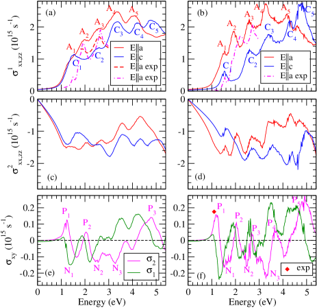
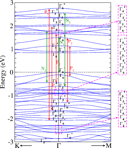
The absorptive parts of the optical conductivity elements (, , and ) are directly related to the dipole allowed interband transitions, as Eqs. (3), (4) and (10) indicate. Therefore, we further analyze the origin of the main features in the , and spectra by considering the symmetries of the involved band states and hence the dipole selection rules (see Supplementary Note B in the SI). Since the spectra of , and for all the considered systems are rather similar, as mentioned above, here we perform the symmetry analysis for ML CrI3 only (see the SI). The scalar-relativistic and relativistic band structures of ML CrI3 with the symmetries of band states at -point labelled, are displayed in Fig. S6 and Fig. 7, respectively. We then assign the main peaks of the and spectra [Fig. 6(b)] to the interband transitions at the -point using the dipole selection rules (see Table S3 in the SI), as presented in Fig. S6. For example, we could relate the A1 peak at 1.5 eV in in Fig. 6(b) to the interband transition from the state at -0.5 eV of the spin-down valence band to the conduction band state at 1.2 eV. Of course, in addition to these dipole-allowed interband transitions at the -point, there are also contributions from different interband transitions at other k-points. It should be noted that, without the SOC, the and band states are doubly degenerate (Fig. S6), and the absorption rates for left- and right-handed polarized lights are the same, thereby resulting in zero contribution to . In the presence of the SOC, the band states split (see Fig. 7) and this gives rise to optical magnetic circular dichroism. For example, we could relate the peak P1 at 1.2 eV in the of Fig. 6(f) to the interband transition from the occupied states at -0.1 eV to the unoccupied state at 1.1 eV (Fig. 7).
For comparison with the available experimental data, we plot in Figs. 6 (a) and (b) the experimental differential reflection spectra (in abitrary units) of bulk and ML CrI3, respectively [7], which are proportional to . Moreover, we also display the of bulk CrI3 derived from the experimental refraction index and extinction coefficent [2] in Fig. 6(a). It can be seen from Fig. 6(a) that twe peaks (A2 and A3 in the experimental of bulk CrI3 [2] agree well with the theoretical ones in both shape and position, although the magnitude of the experimental spectrum is slightly smaller. Moreover, three peaks (A1, A2 and A3) in the experimental differential reflection spectrum of bulk CrI3 [7] also agree very well with the theoretical ones [see Fig. 6(a)]. This indicates that our GGA + calculations could describe the optical properties of bulk CrI3 quite well. Figure 6(b) shows that three peaks (A1, A2 and A3) in the experimental differential reflection spectrum of ML CrI3 [7] are also quite well reproduced by our GGA + calculations. In particular, the position and shape of peak A1 in theoretical and experimental spectra are in good agreement, although theoretical peaks A2 and A3 are red-shifted by about 0.3 eV relative to the experimental ones. Assuming photoluminescence (PL) intensity () is proportional to photoabsorption (), PL circular polarization , i.e., . In Fig. 6(f), the red diamond denotes the estimated this way based on the calculated and experimental for ML CrI3 [7], which agree well with peak P1 in the theoretical spectrum.
Table 1 indicates that the calculated band gap of bulk CrI3 is about 50 % smaller than the experimental value [3]. As usual, we could attribute this significant discrepancy to the known underestimation of the band gaps by the GGA functional where many-body effects especially quasiparticle self-energy correction are neglected. Since Eqs. (3) and (4) indicate that correct band gaps would be important for obtaining accurate optical conductivity and hence magneto-optical effects, we further perform the band structure calculations using the hybrid Heyd-Scuseria-Ernzerhof (HSE) functional [55, 56] which is known to produce improved band gaps for semiconductors (see Supplementary Note C in the SI for the details). The HSE band structures and band gaps are presented in Fig. S7 and Table S4 in the SI, respectively. Indeed, the HSE band gap of bulk CrI3 agrees well with the experimental value [3]. Therefore, we also calculate the optical and magneto-optical properties of bulk and few-layer CrI3 from the GGA + band structures within the scissors correction (SC) scheme [57] using the differences between the HSE and GGA band gaps (Table S4). The optical conductivity spectra calculated with the SC are displayed in Fig. S8 in the SI. Surprisingly, the optical conductivity spectra of bulk and ML CrI3 calculated with the SC are in worse agreement with the corresponding experimental values [7, 2] [see Figs. S8(a), S8(b) and S8(j)]. This could be explained as follows. We notice that bulk CrI3 has an indirect band gap (see Fig. 3). Consequently, the discrepancy in the band gap between theory and experiment in bulk CrI3 could be attributed to the fact that the experimental band gap is the optical one due to direct interband transitions whose energy should be larger than the indirect band gap (see Fig. 7).
3.4 Magneto-optical Kerr and Faraday effects
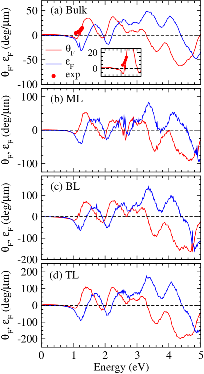
Finally, let us move onto the MO Kerr and Faraday rotational angles calculated from the obtained optical conductivity spectra. To calculate the Kerr angles of the few-layer structures, we also need to know the dielectric constant of the substrate [see Eq. (8)]. Here we assume that the substrate is SiO2 with dielectric constant for all CrI3 multilayers since SiO2 was used in the MOKE experiments [2]. The calculated complex Kerr and Faraday rotation angles as a function of photon energy are presented, respectively, in Figs. 8 and 9 for all the investigated structures. Figures 8 and 9 show that the MO spectra for all the investigated structures except the bulk, are negligible below the band gap of 1.0 eV. Nonetheless, they all become pronounced above 1.0 eV and oscillate as the photon energy increases. We notice that the Kerr rotation () and Kerr ellipticity () of all the structures (Fig. 8) are, respectively, similar to that of the real part () and imaginary part () of the off-diagonal conductivity element (Fig. 6). This could be expected because the Kerr effect and the off-diagonal conductivity element are connected through Eqs. (7) and (8). In fact Eqs. 7 and 8 indicate that the complex Kerr rotation angle would be proportional to the off-diagonal optical conductivity of if the conductivity of the sample and substrate is roughly a constant of photon energy. For the CrI3 multilayers, the dielectric constant of of the SiO2 substrate is a constant and thus the Kerr rotation angle is proportional to the . For bulk CrI3, the Kerr rotation could become large if the , which is in the denominator of Eq. (7), becomes very small. This explains why the Kerr angles of the bulk are still pronounced below 0.5 eV [Fig. 8(a)].
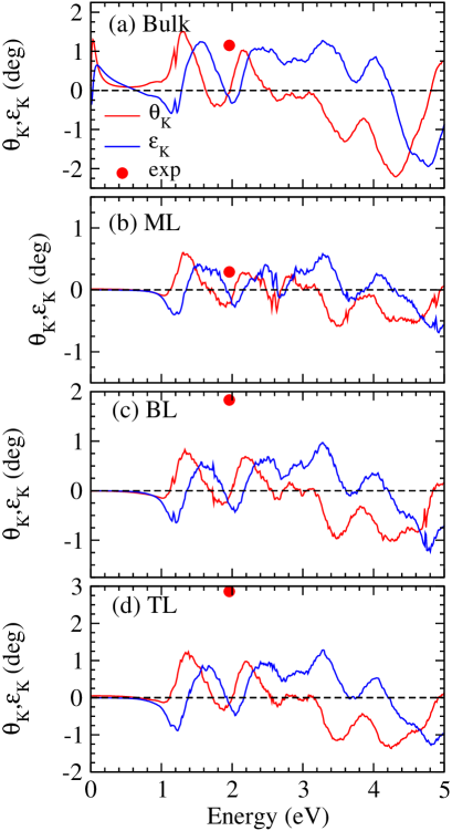
The overall behavior of the MO spectra for all the investigated structures (Figs. 8 and 9) is rather similar, which could be attributed to the weakness of the van der Waals interlayer interaction. Notably, the maximum Kerr rotation angles for all the systems are large. Specifically, the maximum values for bulk, ML, BL and TL CrI3 are, respectively, 1.5, 0.6, 0.8 and 1.2 at 1.3 eV. Kerr ellipticity shows a maximum value of 1.3 at 1.6 eV for the bulk as well as 0.6, 0.9 and 1.2 at 3.3 eV for the ML, BL and TL, respectively. As for the calculated optical conductivities, we notice that the negative peaks also exist in both Kerr rotation and ellipticity spectra. The negative maximum of the Kerr rotation angle occurs at 4.3 eV for the bulk (-2.1) and at 4.2 eV for the TL (-1.3) as well as at 3.3 eV for the ML (-0.5) and 4.2 eV for the BL (-1.0). Similarly, Kerr ellipticity shows the negative maximum near 4.8 eV for the bulk (-1.9) as well as at 4.9 eV for the ML (-0.6) and at 4.8 eV for BL (-1.2) and TL (-1.3). These large Kerr angles and ellipticities indicate that the considered structures would have valuable applications in magneto-optical nanodevices.
To access the application potential of these CrI3 materials for applications, let us now compare their MO properties with several well-known MO materials such as 3 transition metal alloys and compound semiconductors. Among the transition metal alloys, manganese-based pnictides are known to have remarkable MO properties. In particular, MnBi thin films were reported to have a large Kerr rotation angle of 2.3 at 1.84 eV. [46, 58] Pt alloys also possess large Kerr rotations in the range of 0.4-0.5 in FePt and Co2Pt [43] and PtMnSb [59]. In these materials, the strong SOC of heavy Pt atoms was shown to play an important role [60]. For comparison, we note that 3 transition metal multilayers were found to have rather small Kerr rotation angles of 0.06 at 2.2 eV for Fe/Cu multilayer, of 0.16 at 2.5 eV for Fe/Au multilayer [61, 44] and also of 0.06 at 1.96 eV for Co/Au multilayer [62]. Among semiconductor MO materials, diluted magnetic semiconductors Ga1-xMnxAs were reported to show significant Kerr rotation angles of 0.4 near of 1.80 eV [63]. Y3Fe5O12 also exhibits a significant Kerr rotation of 0.23 at 2.95 eV [64]. In strong contrast, the measured Kerr rotation angles of bulk and atomically thin films of Cr2Ge2Te6 are much smaller [1]. For example, the experimental Kerr angle at 0.8 eV is only 0.14 for the bulk, and ranges from 0.0007 in bilayer to 0.002 in trilayer [1]. Overall, the Kerr rotation angles predicted for bulk and multilayer CrI3 here are comparable to these important MO metals and semiconductors. Thus, because of their excellent MO properties, CrI3 structures could have promising applications in, e.g., MO nanosensors and high density MO data-storage devices.
The calculated complex Faraday rotation angles for all the investigated structures are presented in Fig. 9. The main features of the Faraday rotation spectra of the considered structures resemble that of the Kerr rotation spectra (see Fig. 8). Notably, the large Faraday rotation maximum occurs at the photon energy of 2.3 eV for the bulk (36°/m), of 1.4 eV for the ML (50°/m), of 2.3 eV for the BL (75°/m) and TL (108°/m). Faraday ellipticity shows the large maximum near 3.3 eV for the bulk (48°/m), the ML (80°/m), the BL (130°/m) and the TL (170°/m). Also we notice that the large negative maximum exists in both Faraday rotation and ellipticity spectra. For example, the negative maximum of the Faraday rotation occurs at 4.3 eV for the bulk (60°/m) and the TL (-194°/m) as well as at 4.7 eV for the ML (-85°/m) and the BL (-155°/m). Faraday ellipticity shows the large negative maximum near 4.8 eV for all the structures with = -47°/m, -85°/m, -148°/m and -155°/m for the bulk, ML, BL and TL, respectively. For comparison, we notice that the MnBi films are known to possess the largest Faraday rotation angles of 80°/m at 1.77 eV [58, 46]. Ferromagnetic semiconductor Y3Fe5O12 show only small Faraday rotation angles of °/m at 2.07 eV [65]. However, the replacement of Y with Bi considerably enhances the Faraday rotations to 35.0°/m at 2.76 eV [66], thus making Bi3Fe5O12 an outstanding MO material. Clearly, the calculated Faraday angles of the CrI3 multilayers are high compared to that of prominent bulk MO metals such as manganese pnictides.
The Kerr rotation angles of bulk and atomically thin film CrI3 have recently been measured at photon energy of 1.96 eV [2] and they are found to be large (see Fig. 8). If the calculated Kerr rotation spectra are red-shifted by merely 0.2 eV, the measured and calculated values of bulk and ML CrI3 would be in very good agreement, although the experimental values of BL and TL CrI3 are much larger than the corresponding theoretical values (Fig. 8). Furthermore, the measured Faraday rotation angles of bulk CrI3[4] are almost in perfect agreement with our theoretical prediction [see Fig. 9(a)]. We notice that in contrast, the photon energies of the experimental Faraday angles of bulk CrI3[4] differ significantly from that of the theoretical Faraday angles calculated with the scissors correction using the HSE band gap [see Fig. S10(a) in the SI].
4 Conclusion
Summarizing, we have systematically studied magnetism, electronic structure, optical and magneto-optical properties of bulk and atomically thin films of CrI3 by performing extensive GGA + calculations. Firstly, we find that both intralayer and interlayer magnetic couplings are strongly ferromagnetic in all the considered CrI3 structures. Ferromagnetic ordering temperatures estimated based on calculated exchange coupling parameters agree quite well with the measured ones. Secondly, we reveal that all the structures have a large out-of-plane MAE of 0.5 meV/Cr, in contrast to the significantly thickness-dependent MAE in atomically thin films of Cr2Ge2Te6. [26] These large MAEs suppress transverse spin fluctuations in atomically thin CrI3 films and thus stabilize long-range magnetic orders at finite temperatures down to the ML limit. Thirdly, all the structures also exhibit strong MO Kerr and Faraday effects. In particular, in these CrI3 structures, MO Kerr rotations up to 2.6 are found, being comparable to famous MO materials such as ferromagnetic semiconductor Y3Fe5O12 and metal PbMnSb. Calculated MO Faraday rotation angles are also large, being up to 200°/m, and they are comparable to that of best known MO semiconductors such as Y3Fe5O12 and Bi3Fe5O12. Calculated optical conductivity spectra, MO Kerr and Faraday rotation angles agree quite well with available experimental data. In BL CrI3, the interlayer magnetic coupling is found to be layer stacking dependent while the optical and magneto-optical properties are not. Therefore, further experimental determination of the structure of BL CrI3 is needed to resolve why the antiferromagnetic state instead of the predicted ferromagnetic state, is observed. Fourthly, all the structures are found to be single-spin ferromagnetic semiconductors. Finally, calculated MAEs, optical and magneto-optical conductivity spectra of these structures are analyzed in terms of their underlying electronic band structures. Our findings of large out-of-plane MAEs and strong MO effects in these single-spin ferromagnetic semiconducting CrI3 ultrathin films suggest that they will find promising applications in high density semiconductor MO and low-power spintronic nanodevices as well as efficient spin-photovoltaics.
Acknowledgement: V. K. G. and G. Y. G. acknowledges the support by the Ministry of Science and Technology and the National Center for Theoretical Sciences, Taiwan. G. Y. G. also thanks the Academia Sinica and the Kenda Foundation of Taiwan for the supports.
References:
References
- [1] C. Gong, L. Li, Z. Li, H. Ji, A. Stern, Y. Xia, T. Cao, W. Bao, C. Wang, Y. Wang, Z. Q. Qiu, R. J. Cava, S. G. Louie, J. Xia and X. Zhang, Nature 546, 265 (2017).
- [2] B. Huang, G. Clark, E. Navarro-Moratalla, D. R. Klein, R. Cheng, K. L. Seyler, D. Zhong, E. Schmidgall, M. A. McGuire, D. H. Cobden, W. Yao, D. Xiao, P. Jarillo-Herrero and X. Xu, Nature 546, 270 (2017).
- [3] J. F. Dillon Jr. and C. E. Olson, J. Appl. Phys. 36, 1259 (1965).
- [4] J. F. Dillon Jr., H. Kamimura, and J. P. Remeik, J. Phys. Chem. Solids. 27, 1531-1549 (1966)
- [5] J. Suits, IEEE Transactions on Magnetics 8, 95-105 (1972).
- [6] J. F. Dillon Jr., J. Magn. Magn. Mater 84, 213 (1990).
- [7] K. L. Seyler, D. Zhong, D. R. Klein, S. Gao, X. Zhang, B. Huang, E. Navarro-Moratalla, L. Yang, D. H. Cobden, M. A. McGuire, W. Yao, D. Xiao, P. Jarillo-Herrero and X. Xu, Nat. Phys. 14, 277 (2018).
- [8] S. Jiang, J. Shan and K. F. Mak, Nat. Mater., 17, 406 (2018).
- [9] B. Huang, G. Clark, D. R. Klein, D. MacNeill, E. Navarro-Moratalla, K. L. Seyler, N. Wilson, M. A. McGuire, D. H. Cobden, D. Xiao and W. Yao, Nature Nanotechnology 13, 544-548 (2018).
- [10] S. Jiang, L. Li, Z. Wang, K. F. Mak and J. Shan, Nat. Nanotechnolog 13, 549-553 (2018).
- [11] T. Song, X. Cai, M. W.-Y. Tu, X. Zhang, B. Huang, N. P. Wilson, K. L. Seyler, L. Zhu, T. Taniguchi, K. Watanabe, M. A. McGuire, D. H. Cobden, D. Xiao, W. Yao and X. Xu, Science 360, 1214 (2018).
- [12] Z. Wang, I. Gutirrez-Lezama, N. Ubrig, M. Kroner, M. Gibertini, T. Taniguchi, K. Watanabe, A. Imamoğlu, E. Giannini and A. F. Morpurgo, Nature Commun. 9, 2516 (2018).
- [13] D. Zhong, K. L. Seyler, X. Linpeng, R. Cheng, N. Sivadas, B. Huang, E. Schmidgall, T. Taniguchi, K. Watanabe, M. A. McGuire, W. Yao, D. Xiao, K.-M. C. Fu, and X. Xu, Sci. Adv. 3, e1603113 (2017).
- [14] W.-B. Zhang, Q. Qu, P. Zhu and C.-H. Lam, J. Mater. Chem. C 3, 12457 (2015).
- [15] H. Wang, F. Fan, S. Zhu and H. Wu, EPL 3, 12457 (2015).
- [16] D. Torelli and T. Olsen, 2D Mater. 6, 015028 (2019).
- [17] J. L. Lado and J. Fernndez-Rossier, 2D Mater. 4, 035002 (2017).
- [18] N. Sivadas, S. Okamoto, X. Xu, Craig. J. Fennie, D. Xiao, Nano Lett. 18, 7658 (2018).
- [19] P. Jiang, C. Wang, D. Chen, Z. Zhong, Z. Yuan, Z.-Y. Lu, and W. Ji, arXiv:1806.09274 (2018).
- [20] D. Soriano, C. Cardoso, J. Fernndez-Rossier, arXiv:1807.00357v1 (2018).
- [21] S. W. Jang, M. Y. Jeong, H. Yoon, S. Ryee and M. J. Han, arXiv:1809.01388v1 (2018).
- [22] N. Mermin and H. Wagner, Phys. Rev. Lett. 17,1133-1136 (1966).
- [23] P. Jiang, L. Li, Z. Liao, Y. X. Zhao and Z. Zhong, Nano Lett. 18, 3844-3849 (2018).
- [24] J. C. Tung and G. Y. Guo, Phys. Rev. B 76, 094413 (2007).
- [25] G. Y. Guo, W. Temmerman and H. Ebert, J. Phys.: Condens. Matter 3, 8205 (1991).
- [26] Y. Fang, S. Wu, Z.-Z. Zhu and G.-Y. Guo, Phys. Rev. B 98, 125416 (2018).
- [27] V. Antonov, B. Harmon, and A. Yaresko. Electronic structure and magneto-optical properties of solids. Springer Science & Business Media, (2004).
- [28] M. Mansuripur, The Principles of Magneto-Optical Recording (Cambridge Univ. Press, Cambridge, 1995).
- [29] J. P. Castera, in Magneto-optical Devices, Vol. 9 of Encyclopedia of Applied Physics, edited by G. L. Trigg (Wiley-VCH, New York, 1996), p. 133.
- [30] M. A. McGuire, H. Dixit, V. R. Cooper and B. C. Sales, Chem. Mater. 27, 612 (2015).
- [31] G. Kresse and D. Joubert, Phys. Rev. B 59, 1758 (1999).
- [32] G. Kresse and J. Furthmüller, Phys. Rev. B 54, 11169 (1996).
- [33] G. Kresse and J. Furthmüller, Comput. Mat. Sci 6, 15–50 (1996).
- [34] J. P. Perdew, K. Burke, and M. Ernzerhof, Phys. Rev. Lett. 77, 3865 (1996).
- [35] H. T. Jeng, G. Y. Guo and D. J. Huang, Phys. Rev. Lett. 93, 156403 (2004).
- [36] S. L. Dudarev, G. A. Botton, S. Y. Savrasov, C. J. Humphreys and A. P. Sutton, Phys. Rev. B 57, 1505 (1998).
- [37] C. S. Wang and J. Callaway, Phys. Rev. B 9, 4897 (1974).
- [38] W. Feng, G.-Y. Guo, J. Zhou, Y. Yao, and Q. Niu, Phys. Rev. B 92, 144426 (2015).
- [39] B. Adolph, J. Furthmüller and F. Bechstedt, Phys. Rev. B 63, 125108 (2001).
- [40] W. M. Temmerman, P. A. Sterne, G. Y. Guo and Z. Szotek, Molecular Simulations 63, 153 (1989).
- [41] G. Y. Guo, K. C. Chu, D.-s. Wang and C.-g. Wang, Phys. Rev. B 69, 205416 (2004).
- [42] G. Y. Guo and H. Ebert, Phys. Rev. B 50, 10377 (1994).
- [43] G. Y. Guo and H. Ebert, Phys. Rev. B 51, 12633 (1995).
- [44] Y. Suzuki,T. Katayama, S. Yoshida,K. Tanaka and K. Sato, Phys. Rev. Lett. 68, 3355 (1992).
- [45] W. Feng, G.-Y. Guo, and Y. Yao, 2D Mater. 4, 015017 (2016).
- [46] P. Ravindran, A. Delin, P. James,B. Johansson, J. M. Wills, R. Ahuja and O. Eriksson, Phys. Rev.B 59, 15680 (1999).
- [47] N. Samarth, Nature 546, 216 (2017).
- [48] P. M. Oppeneer, J. Magn. Magn. Mater. 188, 275 (1998).
- [49] S. V. Halilov, H. Eschrig, A. Y. Perlov and P. M. Oppeneer, Phys. Rev. B 58, 293 (1998).
- [50] M. Pajda, J. Kudrnovsky, I. Turek, V. Drchal and P. Bruno, Phys. Rev. Lett. 85, 5424 (2000).
- [51] V. Y. Irkhin, A. A. Katanin and M. I. Katsnelson, Phys. Rev. B 60, 1082 (1999).
- [52] T.-Y. Cai, S.-C. Liu, S. Ju, C.-Y. Liu and G.-Y. Guo, Phys. Rev. Appl. 8, 034034 (2017).
- [53] D.-S. Wang, R. Wu and A. J. Freeman, Phys. Rev. B 47, 14932 (1993).
- [54] H. Takayama, K.-P. Bohnen and P. Fulde, Phys. Rev. B 14, 3387 (1976).
- [55] J. Heyd, J. Chem. Phys. 118, 8207 (2003).
- [56] J. Heyd, G. E. Scuseria, and M. Ernzerhof, J. Chem. Phys. 124, 219906 (2006).
- [57] Z. H. Levine and D. C. Allan, Phys. Rev. B 43, 4187 (1991).
- [58] G. Di and S. Uchiyama, Phys. Rev. B 53, 3327 (1996).
- [59] P. Van Engen, K. Buschow, R. Jongebreur, and M. Erman, Appl. Phys. Lett. 42, 202–204 (1983).
- [60] G. Y. Guo and H. Ebert, J. Magn. Magn. Mater. 156, 173 (1996).
- [61] T. Katayama, Y. Suzuki, H. Awano, Y. Nishihara and N. Koshizuka, Phys. Rev. Lett. 60 1426–9 (1988).
- [62] R. Mgy, A. Bounouh, Y. Suzuki, P. Beauvillain, P. Bruno, C. Chpert, B. Lecuyer and P. Veillet, Phys. Rev. B 51 5586–9 (1995).
- [63] R. Lang, W. H. Pascher, H. Krenn, X. Liu and J. K. Furdyna, Phys. Rev. B 72, 024430 (2005).
- [64] S. Tomita, T. Kato, S. Tsunashima, S. Iwata, M. Fujii and S. Hayashi, Phys. Rev. B 96, 167402 (2006).
- [65] T. Boudiar, B. Payet-Gervy, M.-F. Blanc-Mignon, J.-J. Rousseau, M. Le Berre and H. Joisten, J. Magn. Magn. Mater. 284, 77-85 (2004).
- [66] B. Vertruyen, R. Cloots, J. Abell, T. Jackson, R. Da Silva, E. Popova and N. Keller, Phys. Rev. B 78, 094429 (2008).