Physical insights into the operation of a 1-nm gate length transistor based on MoS2 with metallic carbon nanotube gate
Abstract
Low-dimensional materials such as layered semiconductors or carbon nanotubes (CNTs) have been attracting increasing attention in the last decades due to their inherent scaling properties, which become fundamental to sustain the scaling in electronic devices. Inspired by recent experimental results (S.B. Desai, S.R. Madhvapathy, A.B. Sachid, J.P. Llinas, Q. Wang, G.H. Ahn, G. Pitner, M.J. Kim, J. Bokor, C. Hu, H.-S. P. Wong, and A. Javey, Science 354, 99 (2016)), in this work we examined the ultimate performance of of MoS2-channel Field Effect Transistors with 1-nm gate length by means of quantum transport simulations based on Poisson equation and Non-equilibrium Green’s function formalism. We considered uniformly scaled devices, with channel lengths ranging from 5 to 20 nm controlled by a cylindrical gate with a 1-nm diameter, as would be required in realistic integrated circuits. Moreover, we also evaluated the effect of the finite density of states of a carbon nanotube gate on the loss of device performance. We noticed that the sub-threshold swing for all short-channel structures was greater than the ideal limit of thermionic devices and we attributed this to the presence of tunneling currents and gate-drain interactions. We tailored the transistor architecture in order to improve the gate control. We concluded that the limited CNT-channel capacitive coupling poses severe limitations on the operation and thus exploitation of the device.
I Introduction
A recent experimental paper has proposed an intriguing possibility to scale down transistor size in the few-nm regime, consisting in the use of a metallic carbon nanotube (CNT) as the gate electrode Desai et al. (2016) of a field-effect transistor (FET) with a monolayer MoS2 channel. Two-dimensional (2D) crystal semiconductors such as MoS2 have been considered as interesting candidates for substituting silicon as channel material at the very end of the semiconductor roadmap (i.e. beyond the so-called 5-nm semiconductor technology node ITR ; Schwierz, Granzner, and Pezoldt (2015); Fiori et al. (2014); Roy et al. (2014); Collaert et al. (2015); Radisavljevic et al. (2011); Moore (1965)). In fact, differently from bulk semiconductors, the natural atomic confinement of the electrons in such layered structures allow a uniform control of the gate over the channel, thus reducing the so-called short-channel effects (SCE) which strongly hinder the performance of ultra-scaled devices: Chhowalla, Jena, and Zhang (2016) the threshold voltage roll-off, the increase of tunneling currents and the drain-induced-barrier lowering (DIBL)Khanna (2016); Agarwal et al. (2016). Desai et al. Desai et al. (2016) suggest the use of one-dimensional (1D) structures to fulfill the function of the transistor gate as a way to overcome lithography limitations, at least in a laboratory environment. A similar approach, has been also pursued by Cao et al. Cao, Liu, and Banerjee (2016), who demonstrated the use of ultra-thin synthesized cylindrical nanowires with a metallic core conformally coated with an high- oxide Houssa et al. (2006). However, both experimental works consider an extremely long channel which is of course not suitable for large-scale industrial applications. In Desai et al. (2016), the source-to-drain distance is of the order of hundreds of nanometers leading to an almost ideal sub threshold swing ( 65 mV per decade). In addition, metallic CNTs have a low density of states that could lead to degraded electrostatics in the case of short channels. In this work, we investigated the CNT-gate FET concept in order to understand the ultimate performance while scaling the device down to ultra short channel lengths.
II Models and Methods
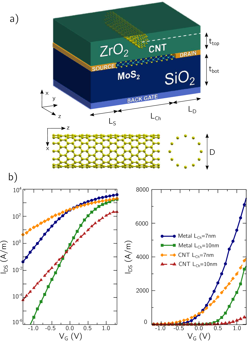
Aiming to determine the operation of the CNT-gated device shown in Fig.1a, we performed fully quantum transport simulations by self-consistently solving Poisson and Schrödinger equations with open boundary conditions at room temperature (300K) Datta (2000) by means of the NanoTCAD ViDES simulation environment Fiori, Iannaccone, and Klimeck (2006); Marin et al. (2018); Nan . Starting from the experimental geometry presented by Desai et al. Desai et al. (2016), we proposed a double gated transistor with a MoS2 monolayer channel of length as shown in Fig.1a. In order to perform the simulations in the best-case scenario, we considered Ohmic contacts by heavily -doping the source and drain regions (=2 nm) to reach a Fermi energy degeneracy of 0.2 eV, with an equivalent electron doping concentration of 4.78 m-2 in these regions. In addition, the channel was electrostatically doped by a metallic back-gate whose voltage () was set to 10 V unless explicitly stated otherwise. The BG is separated from the channel by a SiO2 back insulator with equivalent thickness =10 nm . We embedded the CNT-gate in ZrO2 and placed it on top of the channel, i.e. on the opposite side of the back-gate with respect to the MoS2, setting a distance =5 nm between the center of the CNT and the channel. We modeled both the MoS2 channel and the CNT through a semi-empirical nearest-neighbor tight-binding approximation: the Hamiltonian of the 2D material has been derived from a model for pseudo-hexagonal lattices, as in Agarwal et al. (2015). For the single-walled CNT we have considered a chiral vector guarantying semi-metallic states in the zig-zag configuration Wong and Akinwande (2011). The Non-Equilibrium Green’s functions (NEGF) Datta (2000) are solved independently for the MoS2 channel and the CNT, to obtain the charge density in each material which is later included in the Poisson equation to self-consistently determine the potential in the device. For the sake of comparison, we also designed an alternative device structure, substituting the CNT with a metallic nanowire as top gate: here, differently from the previous scenario, the fixes the potential around the cylindrical gate. Lastly, the transmission coefficient (T) was determined considering 32 transversal modes to perform transport calculations. We then exploited T to compute the current along the MoS2 channel following Landauer’s approach Landauer (1957) in the case of pure ballistic transport, fixing the source-to-drain voltage at =0.5 V.
III Simulation Results
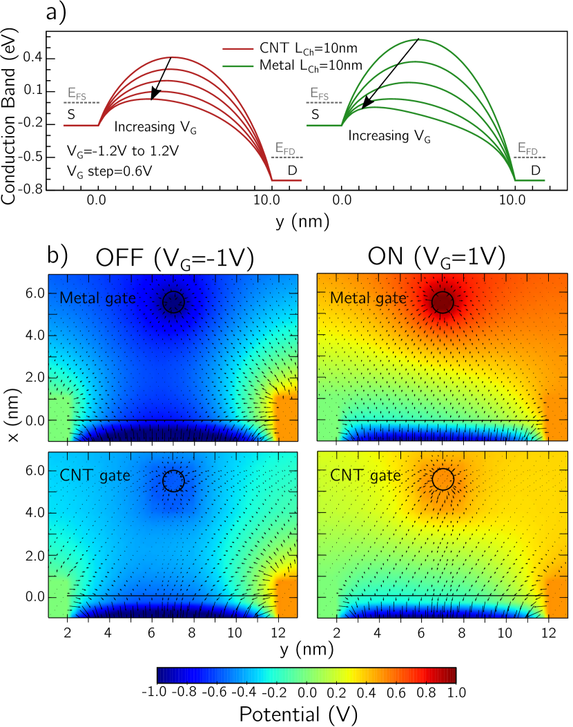
In order to capture the switching behavior and the ultimate performance of a uniformly ultra-scaled device, we will proceed as follows: we will start by examining devices of two different channel lengths with either a CNT or a metallic cylindrical gate; in addition, for the latter configuration we will investigate on the effect of by separating the different current components, and we will conclude by proposing some optimization parameters. We extracted the characteristics for =7 nm and =10 nm gated with a nanotube of =1 nm. The curves, shown in logarithmic and linear scale in Fig. 1b with dashed lines, report a far from the ideal limit of 60 mV/dec reaching at best 300 mV/dec for the longest channel length. The ratio of the ON-current to the OFF-current is less than two orders of magnitude, which means that it does not comply with the specifications for high-performance applications defined by the International Roadmap for Semiconductors (ITRS)ITR . The values were taken at 10-1 A/m and, when not possible, to the lowest value of the current in the considered voltage window, the values were consequently extracted at +0.5 V. To understand the extent to which the finite density of states (DOS) could hinder the characteristics, we replaced the CNT with a cylindrical ideal metallic gate with continuous DOS, as an upper-limit case benchmark. A first observation must be done on the base of the results of the transfer characteristics in Fig.1b comparing simulations with the same and different gate types. If we focus on the longest channel, the improvement with the metallic gate is evident where the lowers from 300 mV/dec to 160 mV/dec; the / as well increases to 400. By looking at the conduction band (CB) profile in the channel as a function of the applied (Fig. 2a), it is possible to notice a worse electrostatic control and less modulation of the carbon nanotube with respect to the metal nanowire gate. Indeed, a of 2.4 V results in a 0.35 eV reduction of the top of the barrier in the former case, half of what is achieved for the latter (0.7 eV). This effect can be also verified by comparing the potential profile and electric field for the different structures. Figure 2b depicts the colormap of the potential for both the OFF- (left) and ON-state (right) in the metal gated (top) and CNT-gated devices (bottom). It is clear from the colormap that already in close proximity of the gate, the effective potential and electric field are significantly reduced when using a CNT. A reasonable explanation can be found in the semi-metallic nature of the carbon nanotube, i.e. its lack of a bandgap and its low DOS: less charge on the gate translates into fewer carriers in the MoS2 channel. In other words, the quantum capacitance of the CNT, added in series to the oxide capacitance , reduces the total gate capacitance .
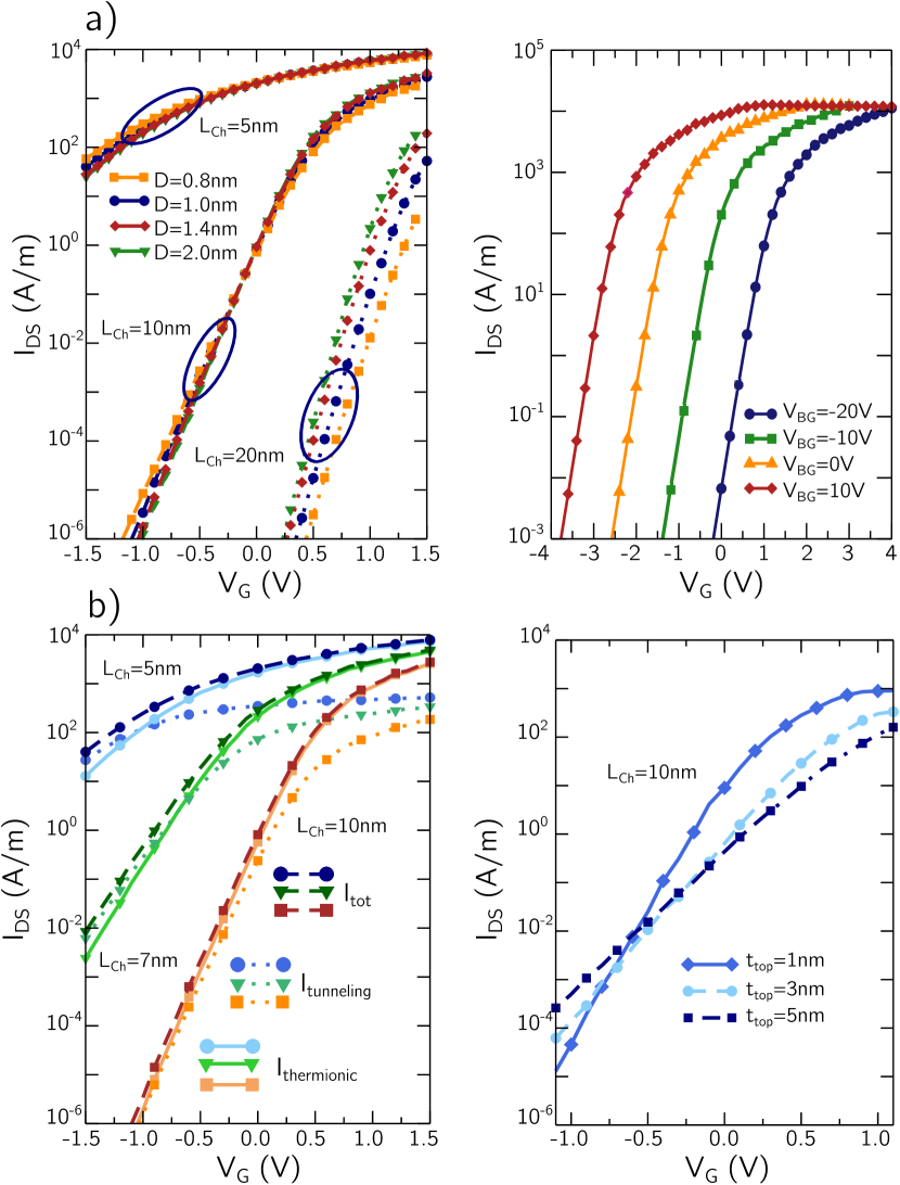
If on the one hand materials properties can explain the limited channel control, on the other hand they alone cannot fully justify a so far from the ideal. In Fig. 3a the curves for various nanowire gate diameters (from =0.8 nm to =2.0 nm) are presented in semi-logarithmic scale, grouped as function of the different channel lengths (=5 nm, 10 nm, 20 nm). Once the finite DOS limitation is removed, it becomes clear that the channel length is a major parameter in determining the device performance: the worsens from 105 mV/dec for =20 nm to 160 mV/dec for =10 nm and finally to 340 mV/dec for =5 nm, whereas the influence of the diameter is almost completely negligible. For what concerns the backgate voltage, as can be seen in Fig. 3a (right panel) it only leads to a rigid shift of the curves, as a result of the different induced charge density, while is not altered. To gain a better insight into the non-ideal behavior of the MOSFETs, we split the output current of metal-gated transistors in the thermionic and tunneling components (Fig. 3b, left panel). The latter refers to electrons having energies lower than the top of the barrier which can tunnel through the barrier if this is sufficiently short: the smaller the (below 10 nm) the higher the tunneling current. In fact, strong SCEs limit both CNT-gated and metal-gated configurations, reasonably as a result of the greater influence of the contacts on the channel region which interferes with the gate control. Nonetheless, little improvements can be obtained in the overall behavior of the initial structure (Fig. 1a) by carefully tuning the device electrostatics. For instance, we reduced the top ZrO2 thickness from 5 nm to 3 nm and pushed it even to a technologically premature 1 nm. The right panel of Fig. 3b reports the characteristics for the three different cases and the reduction in the s from 317 mV/dec, 256 mV/dec, to 172 mV/dec goes together with the decreasing of the oxide thickness.
IV Conclusion
In this work we investigated the performance of field-effect transistors with MoS2 channel and with a gate electrode consisting of a metallic CNT of diameter 1 nm via fully ballistic quantum transport simulations. We then analyzed the detrimental impact of the finite density of states of the nanotube by comparing the CNT-gated devices with those with an ideal metallic cylinder of the same dimension, representing an upper-limit case scenario. We were able to notice larger values of for short-channel structures compared to the ideal 60 mV per decade of thermionic devices, which negatively affect the switching behavior of the transistors. We attributed the poor gate control to SCEs such as the presence of tunneling currents and to gate-drain interactions. Finally, in order to optimize the initial CNT-gated configuration, we indicated few parameters to tune such as the top oxide thickness able to reduce the and improve the characteristics, unlike the gate diameter and the back-gate voltage.
The authors acknowledge the support from the Graphene Flagship (No. 785219). The authors gratefully acknowledge fruitful discussions with S.B. Desai and A. Javey
References
- Desai et al. (2016) S. B. Desai, S. R. Madhvapathy, A. B. Sachid, J. P. Llinas, Q. Wang, G. H. Ahn, G. Pitner, M. J. Kim, J. Bokor, C. Hu, H.-S. P. Wong, and A. Javey, Science 354, 99 (2016), doi: 10.1126/science.aah4698.
- (2) “International Technology Roadmap for Semiconductors (ITRS),” http://www.itrs2.net/.
- Schwierz, Granzner, and Pezoldt (2015) F. Schwierz, R. Granzner, and J. Pezoldt, Nanoscale , 8261 (2015), doi: 10.1039/C5NR01052G.
- Fiori et al. (2014) G. Fiori, F. Bonaccorso, G. Iannaccone, T. Palacios, D. Neumaier, A. Seabaugh, S. K. Banerjee, and L. Colombo, Nature Nanotechnology 9, 768 (2014), doi: 10.1038/nnano.2014.207, arXiv:arXiv:1411.2774v2 .
- Roy et al. (2014) T. Roy, M. Tosun, J. S. Kang, A. B. Sachid, S. B. Desai, M. Hettick, C. C. Hu, and A. Javey, ACS Nano 8, 6259 (2014), doi: 10.1021/nn501723y.
- Collaert et al. (2015) N. Collaert, A. Alian, H. Arimura, G. Boccardi, G. Eneman, J. Franco, T. Ivanov, D. Lin, R. Loo, C. Merckling, J. Mitard, M. A. Pourghaderi, R. Rooyackers, S. Sioncke, J. W. Sun, A. Vandooren, A. Veloso, A. Verhulst, N. Waldron, L. Witters, D. Zhou, K. Barla, and A. V. Thean, “Ultimate nano-electronics: New materials and device concepts for scaling nano-electronics beyond the Si roadmap,” (2015), doi: 10.1016/j.mee.2014.08.005.
- Radisavljevic et al. (2011) B. Radisavljevic, A. Radenovic, J. Brivio, V. Giacometti, and A. Kis, Nature Nanotechnology 6, 147 (2011), doi: 10.1038/nnano.2010.279, arXiv:0402594v3 [arXiv:cond-mat] .
- Moore (1965) G. E. Moore, Electronics 38, 114 (1965).
- Chhowalla, Jena, and Zhang (2016) M. Chhowalla, D. Jena, and H. Zhang, Nature Reviews Materials 1, 16052 (2016), doi: 10.1038/natrevmats.2016.52.
- Khanna (2016) V. K. Khanna, “Short-channel effects in mosfets,” in Integrated Nanoelectronics: Nanoscale CMOS, Post-CMOS and Allied Nanotechnologies (Springer India, New Delhi, 2016) pp. 73–93.
- Agarwal et al. (2016) T. Agarwal, B. Sorée, I. Radu, P. Raghavan, G. Fiori, G. Iannaccone, A. Thean, M. Heyns, and W. Dehaene, Applied Physics Letters 108, 023506 (2016), doi: 10.1063/1.4939933, https://doi.org/10.1063/1.4939933 .
- Cao, Liu, and Banerjee (2016) W. Cao, W. Liu, and K. Banerjee, in 2016 IEEE International Electron Devices Meeting (IEDM) (IEEE, 2016) pp. 14.7.1–14.7.4, doi: 10.1109/IEDM.2016.7838419.
- Houssa et al. (2006) M. Houssa, L. Pantisano, L.-A. Ragnarsson, R. Degraeve, T. Schram, G. Pourtois, S. De Gendt, G. Groeseneken, and M. Heyns, Materials Science & Engineering R, Reports 51, 37 (2006).
- Datta (2000) S. Datta, Superlattices and Microstructures 28, 253 (2000), doi: 10.1006/spmi.2000.0920.
- Fiori, Iannaccone, and Klimeck (2006) G. Fiori, G. Iannaccone, and G. Klimeck, IEEE Transactions on Electron Devices 53, 1782 (2006), doi: 10.1109/TED.2006.878018.
- Marin et al. (2018) E. G. Marin, M. Perucchini, D. Marian, G. Iannaccone, and G. Fiori, IEEE Transactions on Electron Devices 65, 4167 (2018), doi: 10.1109/TED.2018.2854902.
- (17) “NanoTCAD ViDES,” http://vides.nanotcad.com/vides/.
- Agarwal et al. (2015) T. Agarwal, D. Yakimets, P. Raghavan, I. Radu, A. Thean, M. Heyns, and W. Dehaene, IEEE Transactions on Electron Devices 62, 4051 (2015), doi: 10.1109/TED.2015.2491021.
- Wong and Akinwande (2011) H.-S. P. Wong and D. Akinwande, Carbon Nanotube and Graphene Device Physics (Cambridge University Press, 2011) p. 251.
- Landauer (1957) R. Landauer, IBM Journal of Research and Development 1, 223 (1957), doi: 10.1147/rd.13.0223.