Nanobenders: efficient piezoelectric actuators for widely tunable nanophotonics at CMOS-level voltages
Abstract
Tuning and reconfiguring nanophotonic components is needed to realize systems incorporating many components. The electrostatic force can deform a structure and tune its optical response. Despite the success of electrostatic actuators, they suffer from trade-offs between tuning voltage, tuning range, and on-chip area. Piezoelectric actuation could resolve all these challenges. Standard materials possess piezoelectric coefficients on the order of , suggesting extremely small on-chip actuation using potentials on the order of one volt. Here we propose and demonstrate compact piezoelectric actuators, called nanobenders, that transduce tens of nanometers per volt. By leveraging the non-uniform electric field from submicron electrodes, we generate bending of a piezoelectric nanobeam. Combined with a sliced photonic crystal cavity to sense displacement, we show tuning of an optical resonance by and between ( linewidths) with only . Finally, we consider other tunable nanophotonic components enabled by nanobenders.
Complete and low-power control over the phase and amplitude of light fields remains a major challenge in integrated photonics. Optical components providing such control are essential in systems being developed for optical computing, signal processing, sensing, and imaging Miller (2017); Hamerly et al. (2019); Pai et al. (2019). Tuning the optical response of an element entails changing its refractive index by, for example, modifying its temperature, imposing electric fields, or mechanically deforming it. Among these, mechanical deformations have the advantage of being essentially lossless, requiring no static power consumption, and possessing an enormous tuning range and cryogenic compatibility Midolo et al. (2018); Safavi-Naeini et al. (2019). Nano-opto-electro-mechanical (NOEM) devices Zheludev and Plum (2016); Midolo et al. (2018) have thus been pursued and demonstrated, to realize switches and couplers for classical and quantum light Van Acoleyen et al. (2012); Han et al. (2015); Seok et al. (2016); Papon et al. (2019); Haffner et al. (2019), resonant and static electro-optomechanical tuning and electro-optical transduction Perahia et al. (2010); Winger et al. (2011); Bagci et al. (2014); Andrews et al. (2014); Pitanti et al. (2015); Grutter et al. (2018); Bekker et al. (2018).
An efficient NOEM device solves two problems simultaneously. It is an optical device whose properties are exceptionally sensitive to mechanical deformations. It is also an electromechanical device where a modest voltage can induce large deformations. State-of-the-art optomechanical cavities routinely achieve coupling coefficients in excess of , and largely satisfy the former requirement. It is more-so the latter requirement of large voltage-induced displacement, which has remained a formidable challenge in this context. Here, two approaches present themselves: electrostatic and piezoelectric forces. Electrostatic forces are generated by the voltage-induced polarization in a material. They do not require any special material property and have been previously used to implement a variety of NOEM systems. However, electrostatic tuning is limited in terms of the achievable tunability and sensitivity due to a trade-off between the generated forces (inversely proportional to capacitor plate spacing) and tuning range (proportional to capacitor plate spacing). Moreover, the quadratic relationship between the induced force and the voltage, and pull-in effect complicate tuning. The piezoelectric effect, which relies on the built-in polarization of a material, has the potential to address all these challenges. There, the displacement-voltage relationship is linear and bidirectional, and is free from the pull-in effect and force/range trade-off. This has led to efforts Hosseini et al. (2015); Tian et al. (2018); Jin et al. (2018); Stanfield et al. (2019) to implement piezo-optomechanically tunable cavities and waveguides and resulted, for example, in demonstrations of cavity wavelength tuning coefficients ranging from 0.1 to 30 pm/V Tian et al. (2018); Jin et al. (2018); Stanfield et al. (2019).
In this work, by considering the interplay between non-uniform electric fields and transverse components of the piezoelectric tensor , we discover an actuation mechanism specific to nanoscale piezoelectric actuators that leads to a two-order-of-magnitude increase in achievable displacements. We propose and demonstrate a compact () and geometrically isolated actuator, which we call a “nanobender”, composed of monolithic metal electrodes on a single layer of a thin-film piezoelectric. The displacement of the nanobender scales quadratically with its length and can be as large as for .
The enormous sensitivity and tuning range achieved in these nanobenders allow us to achieve a significant breakthrough in NOEM performance. We demonstrate a “zipper” optomechanical cavity Eichenfield et al. (2009); Leijssen and Verhagen (2015) actuated by four nanobenders that deform the structure to tune the optical resonance wavelength by . With a tuning speed approaching , and a tuning range of with around , we show single-mode tuning across the full telecom C-band with a CMOS voltage. We further show that the displacement generated by the nanobenders is sufficiently large to “zip” and “unzip” the zipper cavity, reversibly manipulating the mechanical mode structure of nanomechanical resonators with switchable contact forces.
Results
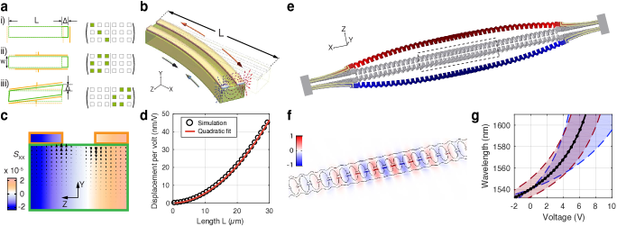
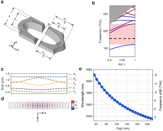
Operating principle of a piezoelectric nanobender. Consider a slab of piezoelectric material sandwiched between two electrodes that are separated by a length and have a potential difference of (Fig. 1a-i). The piezoelectric property of a material is represented by its charge piezoelectricity tensor , a third-rank tensor that relates strain to electric field inside a material (). The terms (Voigt notation) couple to , for , causing compressional/tensile strain to build up in the direction of the electric field. This leads to a displacement . Considering that in standard piezoelectric materials such as aluminum nitride (AlN) and lithium niobate (LN) Weis and Gaylord (1985); Guy et al. (1999), such a transducer would only generate displacements at the atomic scale for voltages which are easily produced by CMOS circuits.
The above expression also shows that the generated displacement does not depend on the size of the transducer. This applies to any piezoelectric actuator. We write the constitutive relation between the strain and the electric field , as where is the displacement field and is the electric potential distribution for a given actuator geometry, applied voltage and boundary conditions. If the geometry of both the actuator and the boundary conditions are scaled by a factor while keeping the same applied voltage, then and are solutions to the new equations. In other words, the magnitude of the displacement stays constant as the actuator is shrunk leading to an increase in relative displacement that favors smaller actuators.
As illustrated above, the diagonal elements of , give rise to tens of picometers of displacement at a potential of around one volt. A much larger displacement can be generated with transverse () components (Fig. 1a-ii). In this situation, the potential gives rise to an electric field across the width , which generates strain along the length of the beam. This leads to a displacement , where we have defined the aspect ratio of the actuator . Compared to the previous case, the displacement is enhanced by . However, reaching with one volt still requires , roughly on the same order as that of a long strand of human hair, or sheet of paper, making it impractical.
Is there a configuration that results in a displacement which scales faster than linear with ? Bending of a beam generates a displacement proportional to , where contraction occurs in one half of the beam and expansion in the other half. Looking back to the corresponding electric field , we recognize that bending can be actuated by flipping the direction of across the width of the beam. Assuming that the derivative of the field is constant across the width of the beam ( is transverse to the beam), the end-point displacement can be approximated by (supplementary information)
| (1) |
We see that the displacement in this case is enhanced by the square of the aspect ratio . The required for is drastically decreased to a practical value . As an example, such a non-uniform field on a wide beam with length would enable actuation of displacement per volt – a displacement on the same order as the width of the beam. We emphasize that the nanoscale aspect of the nanobender is important for achieving such a large relative displacement. By the scale-invariance arguments above, a larger structure would generate the same displacement, leading to a less appreciable relative motion.
A strongly inhomogeneous field is naturally generated by the fringing fields of a submicron-scale electrode configuration. We consider a simple device, which we call the nanobender, where a pair of parallel electrodes lies on the top surface of a beam made of a thin piezoelectric LN film. For a beam oriented along crystal axis , the inhomogeneous field induces a varying strain and results in bending of the beam (Fig. 1b) via the piezoelectric tensor element . For -cut LN where the crystal axis is perpendicular to the chip, this bending gives rise to an in-plane displacement that scales quadratically with . Finite-element simulations Inc. of the nanobender are shown in Fig. 1c. The simulated (arrowheads) changes sign along , causing expansion in one half of the beam and contraction in the other. For all the simulations and experiments, we use a nanobender width nm, LN thickness nm, electrode width nm, electrode-electrode gap nm and an aluminum electrode thickness nm. A more detailed study of how these parameters affect nanobender performance is presented in the supplementary information. Once the nanobender’s cross section is fixed, the length ultimately determines the maximum displacement generated at the end of the beam. Through simulations (Fig. 1d) we are able to confirm the quadratic length-displacement relationship in equation (1). The simulated displacement along the other two directions are more than one order of magnitude smaller.
Actuation that induces bending is commonly adopted by macroscopic piezoelectric actuators, realizing displacement per volt values similar to the nanobenders ( with ) Safari and Akdogan (2008). In these actuators, a non-uniform strain distribution is achieved by combining multiple layers of different materials, some of which are piezoelectric. However, such an approach is impractical at the nanoscale and difficult to realize in an integrated platform, especially for in-plane actuation. Remarkably, electrostatic forces can also be used to generate bending with large travel Conrad et al. (2015), though scaling actuators down to a few microns is challenging, and current demonstrations require much larger footprints for similar displacements ( for ).
Integration with a zipper cavity. By integrating the nanobender with a nanophotonic “zipper” cavity Eichenfield et al. (2009); Leijssen and Verhagen (2015) on the thin-film LN material platform, we demonstrate its potential for realizing photonic devices with wide low-voltage tunability. A zipper cavity is a sliced photonic crystal consisting of two nano-patterned beams separated by a gap that confines an optical resonance. The component of the fundamental optical cavity mode is plotted in Fig. 1f. Due to the sub-wavelength confinement of the mode, the resonance wavelength of the cavity is strongly dependent on the gap between the two beams (supplementary information). A voltage applied to the nanobenders moves the two halves of the zipper cavity (Fig. 1e), tuning the optical resonance wavelength. In Fig. 1g we present the simulated voltage-wavelength tuning curve. The tuning curve is nonlinear due to the large changes in – a smaller increases the optical mode confinement and optomechanical coupling, increasing the slope of the tuning curve.
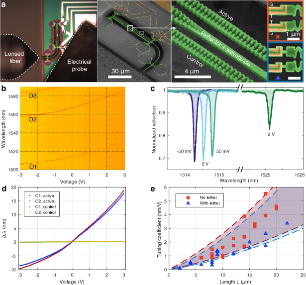
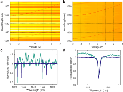
To couple light into the device, we use an edge coupling scheme where a lensed fiber is aligned to a tapered waveguide (Fig. 2a). Light is guided to a reflector and evanescently couples to both an active and a control zipper cavity. The reflection spectrum of the device is recorded for all subsequent measurements (see methods). The bender-zipper cavity is positioned such that the nanobenders are parallel to the crystal axis, necessary for the nanobenders to operate as designed. We also fabricate and measure a device with nanobenders perpendicular to the crystal axis and measure two orders of magnitude lower tuning (see supplementary information). We attach the nanobenders to the zipper cavity with and without narrow tethers and measure larger tuning in the untethered devices (highlighted in blue and red in Fig. 2a,e). To apply a voltage to the nanobenders, we use electrical probes to make contact with on-chip aluminum pads.
We apply voltages to the nanobenders in steps of mV and obtain the reflection spectrum for each voltage (Fig. 2b). We observe wavelength tuning for three different optical modes of the active cavity. No tuning for the control cavity is observed. Additionally the linear wavelength-voltage relationship around V indicates that tuning originates from the piezoelectric effect, in contrast to electrostatic, thermo-optical, and thermo-mechanical tuning. Reflection spectra near the fundamental optical mode around V and at V are shown in Fig. 2c. The linewidth of is around pm corresponding to a quality factor of . The linewidth is limited by thermal mechanical broadening and decreases by almost an order of magnitude at K (supplementary information). The shallower dip at V is due to a decrease of the external coupling rate as the separation between the zipper cavity and the coupling waveguide is increased by actuation of the nanobender. It may be possible to compensate for this effect by using a secondary nanobender on the coupling waveguide or actuate the two halves of the zipper cavity independently. In Fig. 2d we show the extracted resonance wavelength shift versus DC voltage for and of the active zipper cavity. We can tune over tens of nanometers with CMOS-level voltages, corresponding to hundreds of optical linewidths. We perform a linear fit on this tuning curve for small voltages ( V) and obtain a tuning coefficient quantifying the change in wavelength per volt of nm/V. All tuning coefficients are reported at V.
We also investigate how tuning coefficient scales with nanobender length (Fig. 2e). For this purpose we fix all other parameters within fabrication imperfections which mostly affect . More than devices with different are measured. As expected, the zipper cavities with longer nanobenders tune more. The tuning coefficients are higher on devices without the tethers. This is partly supported by simulations. Hence optimizing the way nanobenders are attached is important for composite mechanical systems.
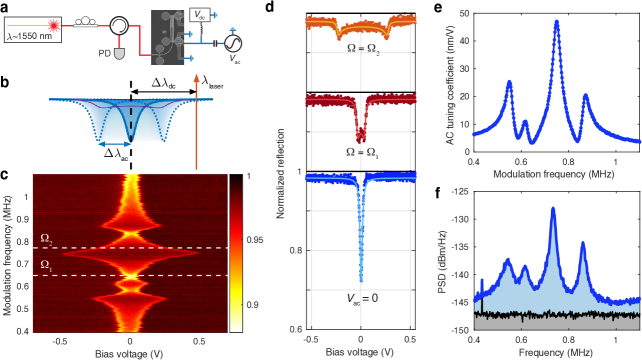
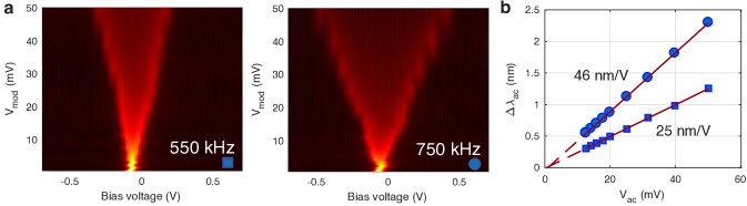
Modulation speed of the bender-zipper cavity. In addition to slowly tuning the bender-zipper cavity using a DC voltage, we also apply a small AC voltage. This allows us to learn about the AC modulation strength as well as the mechanical resonance frequencies of the bender-zipper device. As shown in Fig. 3a, the total voltage applied on the nanobenders is where is the modulation frequency. These voltages lead to wavelength shifts of the cavity given by where is a phase offset. In the DC measurements, we sweep the laser wavelength across the resonance of the cavity. For AC measurements, we instead fix the wavelength of the laser and sweep the cavity using the bias voltage (see Fig. 3b), while using the AC voltage to modulate the cavity resonance. The measurement result is the convolution of the cavity’s Lorentzian lineshape with the probability distribution that samples the sinusoidally modulated cavity center frequency.
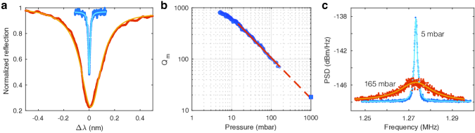
Sweeping the modulation frequency (Fig. 3c), we observe that the AC tuning coefficient is enhanced at certain frequencies close to MHz. These correspond to the mechanical resonances of the bender-zipper device (supplementary information). The data was taken with mV. Cut-lines of the dataset are shown in Fig. 3d, both off-resonance () and close to resonance (). We also show a measurement without AC modulation where we recover a simple Lorentzian. We fit the reflection spectra to extract the AC tuning coefficient and plot it as a function of the modulation frequency (Fig. 3e). Consequently, we are not only able to observe the mechanical resonance frequencies of the system but also directly extract the strength of the modulation. On mechanical resonance, the tuning coefficient is enhanced by a factor , amounting to nm/V. This corresponds to mV. As expected, the frequency dependence of the AC tuning coefficient closely matches with the thermal-mechanical spectrum (Fig. 3f). We obtain the thermal-mechanical spectrum by detuning the laser from the cavity by around half a linewidth where the cavity frequency fluctuations are transduced to intensity fluctuations that we detect with a high speed detector and record on a real-time spectrum analyzer. The mechanical quality factor is relatively low due to air damping. This is verified by measurements in low pressure conditions which show several orders of magnitude enhancement in (supplementary information). Thus, modulation experiments at low pressures could enable even larger resonant AC tuning coefficients (over a smaller bandwidth), reducing to .
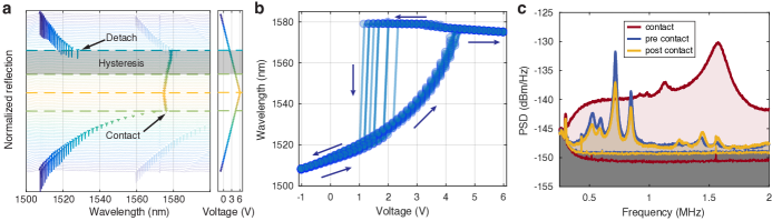
Mechanical contact and hysteresis. We have shown that tens of millivolts are sufficient to tune the optical cavity by more than its linewidth. The small gap and large displacement per volt, taken together, means that the two halves of the zipper touch for voltages on the order of V.
We demonstrate continuous wavelength tuning of a bender-zipper cavity with by reducing the gap between the two halves of the zipper down to the point when they come into contact (Fig. 4a). Focusing on the fundamental mode , we measure a tuning range of nm with V. To the best of our knowledge, this is the largest tuning range demonstrated for an on-chip optical cavity using CMOS-level voltages. From the initial gap size, we infer a displacement actuation of nm/V from each pair of nanobenders. After the contact, the tuning stops regardless of increasing voltage.
As we begin decreasing the voltage, the resonance wavelength shifts ten times less than before the contact because the zipper halves are stuck. We find that the voltage needs to be reduced lower than the contact voltage for the tuning to be restored. This hysteresis is likely due to the van der Waals force that keeps the zippers attached. When we further decrease the voltage, the nanobenders exert a force opposite in direction which eventually manage to detach the zippers. The whole process is reversible as the mode recovers its original wavelength after detaching.
The hysteresis behavior could be applied as an optical memory which necessitates hysteresis for functioning. We test the reliability of the hysteresis loop by repeating the contact-detach process. In Fig. 4b we show nine successive contact-detach cycles, which were preceded by cycles. The hysteresis loop is apparent and there is relatively good overlap between the cycles. However the voltage at which the zippers detach is not consistent across cycles and drifts to lower voltages. After several cycles, the nanobenders are not able to get the zippers to detach (not shown here) although we have found that applying a short AC pulse on mechanical resonance is able to detach them reliably, acting as a reset operation. After the reset, for several cycles the zippers are again able to detach with a DC voltage. The reason for this behavior will be subject to future investigations.
In Fig. 4c we show measurements of the thermal power spectral density of the bender-zipper cavity before contact, during contact and after detaching. We see a clear difference in the spectra between the detached zipper and the attached one. In the latter case, the lateral relative motion between the two halves of the zipper cavity is effectively suppressed. The higher noise floor measured during the contact is likely from laser phase noise, which is more efficiently transduced due to a narrower optical linewidth. We are thus able to reversibly modify both the optical and mechanical properties of the zipper cavity using the nanobenders.
Discussion
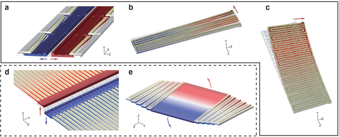
Beyond the demonstrated tunable bender-zipper nanophotonic cavity, various tunable nanophotonic components including phase shifters and couplers can be realized with nanobenders. We show some examples in Fig. 5. An array of nanobenders connected in parallel to a sliced ridge waveguide acts as a phase shifter. The two halves of the sliced ridge waveguide shift towards or away from each other, effectively tuning the index of the fundamental TE mode Midolo et al. (2018); Papon et al. (2019).
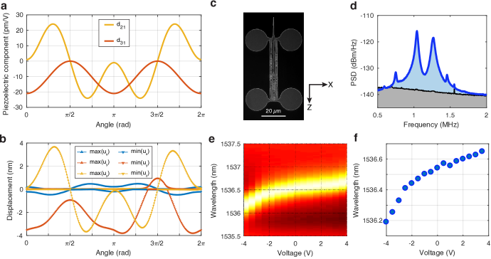
For applications where a large displacement per volt is desired, a series of nanobenders could be connected in a zig-zag fashion to reduce the length of the occupied region. The direction of the actuated displacement can be controlled by engineering the aspect ratio of the zig-zag pattern (supplementary information). We show one zig-zag bender with four nanobenders and one with twenty nanobenders (Fig. 5b & c). They have similar simulated displacement per volt of and actuated along two different directions.
Until now, we have considered nanobenders fabricated with -cut LN, where the dominant displacement is in-plane, parallel to the surface of the chip. Nanobenders with identical geometry fabricated on -cut LN and parallel to the crystal axis, would generate vertical bending (supplementary information). As shown in Fig. 5(d), these nanobenders can be connected in parallel, for extra structural support, and used to implement a tunable optical coupler Han et al. (2015); Seok et al. (2016). Moreover, when connected in a zig-zag fashion, a twist is accumulated along the zig-zag. This can be applied to tilt a mirror attached to the end of the zig-zag structure (Fig. 5e). The rotation angle per volt, actuation speed and device footprint of this type of piezoelectric micro-mirror are comparable to those of the widely used Digital Mirror Devices (DMD) Dudley et al. (2003).
To summarize, we have introduced and implemented the nanobender, a component capable of generating tens of nanometers of displacement per volt using the piezoelectric effect at the submicron scale. We have experimentally shown tuning of a photonic resonator over the entire telecom C-band with CMOS-level voltages and proposed several new photonic devices that leverage the capabilities of the nanobender. Greater control over photonic and phononic devices on the promising thin-film lithium niobate material platform complements on-going efforts to implement ultra-low-power modulation Wang et al. (2018a); Zhang et al. (2019), nonlinear nanophotonic circuits Wang et al. (2018b); Chen et al. (2019); Lu et al. (2019), quantum nanomechanics Arrangoiz-Arriola et al. (2018, 2019), and microwave optomechanical transduction Jiang et al. (2019a); Shao et al. (2019); Dahmani et al. (2019); Jiang et al. (2019b). For emerging quantum technologies that require frequency matching nanophotonic cavities to quantum dots, color centers or rare-earth-doped crystals Englund et al. (2005); Faraon et al. (2011); Zhong et al. (2015), our approach benefits from being able to operate at cryogenic temperatures, while avoiding electric fields, excess carriers, and adsorbed gas molecules, all of which have deleterious effects on the cavity or emitter. Finally, the linear voltage-displacement nature of the piezoelectric effect, the ability to engineer the frequency response and the possibility of dense integration with full electrical access make the nanobenders appealing for sensing Arlett et al. (2011); Krause et al. (2012); Bagci et al. (2014); Mason et al. (2019) and energy harvesting Wang and Song (2006); Wang (2008).
References
- Miller (2017) D. A. Miller, Journal of Lightwave Technology 35, 346 (2017).
- Hamerly et al. (2019) R. Hamerly, L. Bernstein, A. Sludds, M. Soljačić, and D. Englund, Physical Review X 9, 021032 (2019).
- Pai et al. (2019) S. Pai, I. A. Williamson, T. W. Hughes, M. Minkov, O. Solgaard, S. Fan, and D. A. Miller, arXiv preprint arXiv:1909.06179 (2019).
- Midolo et al. (2018) L. Midolo, A. Schliesser, and A. Fiore, Nature nanotechnology 13, 11 (2018).
- Safavi-Naeini et al. (2019) A. H. Safavi-Naeini, D. Van Thourhout, R. Baets, and R. Van Laer, Optica 6, 213 (2019).
- Zheludev and Plum (2016) N. I. Zheludev and E. Plum, Nature nanotechnology 11, 16 (2016).
- Van Acoleyen et al. (2012) K. Van Acoleyen, J. Roels, P. Mechet, T. Claes, D. Van Thourhout, and R. Baets, IEEE Photonics Journal 4, 779 (2012).
- Han et al. (2015) S. Han, T. J. Seok, N. Quack, B.-W. Yoo, and M. C. Wu, Optica 2, 370 (2015).
- Seok et al. (2016) T. J. Seok, N. Quack, S. Han, R. S. Muller, and M. C. Wu, Optica 3, 64 (2016).
- Papon et al. (2019) C. Papon, X. Zhou, H. Thyrrestrup, Z. Liu, S. Stobbe, R. Schott, A. D. Wieck, A. Ludwig, P. Lodahl, and L. Midolo, Optica 6, 524 (2019).
- Haffner et al. (2019) C. Haffner, A. Joerg, M. Doderer, F. Mayor, D. Chelladurai, Y. Fedoryshyn, C. I. Roman, M. Mazur, M. Burla, H. J. Lezec, V. A. Aksyuk, and J. Leuthold, Science 864, 860 (2019).
- Perahia et al. (2010) R. Perahia, J. Cohen, S. Meenehan, T. M. Alegre, and O. Painter, Applied Physics Letters 97, 191112 (2010).
- Winger et al. (2011) M. Winger, T. Blasius, T. M. Alegre, A. H. Safavi-Naeini, S. Meenehan, J. Cohen, S. Stobbe, and O. Painter, Optics express 19, 24905 (2011).
- Bagci et al. (2014) T. Bagci, A. Simonsen, S. Schmid, L. G. Villanueva, E. Zeuthen, J. Appel, J. M. Taylor, A. Sørensen, K. Usami, A. Schliesser, et al., Nature 507, 81 (2014).
- Andrews et al. (2014) R. W. Andrews, R. W. Peterson, T. P. Purdy, K. Cicak, R. W. Simmonds, C. A. Regal, and K. W. Lehnert, Nature Physics 10, 321 (2014).
- Pitanti et al. (2015) A. Pitanti, J. M. Fink, A. H. Safavi-Naeini, J. T. Hill, C. U. Lei, A. Tredicucci, and O. Painter, Optics express 23, 3196 (2015).
- Grutter et al. (2018) K. E. Grutter, M. I. Davanço, K. C. Balram, and K. Srinivasan, APL Photonics 3, 100801 (2018).
- Bekker et al. (2018) C. Bekker, C. G. Baker, R. Kalra, H.-H. Cheng, B.-B. Li, V. Prakash, and W. P. Bowen, Optics express 26, 33649 (2018).
- Hosseini et al. (2015) N. Hosseini, R. Dekker, M. Hoekman, M. Dekkers, J. Bos, A. Leinse, and R. Heideman, Optics express 23, 14018 (2015).
- Tian et al. (2018) H. Tian, B. Dong, M. Zervas, T. J. Kippenberg, and S. A. Bhave, in CLEO: Science and Innovations (Optical Society of America, 2018) pp. SW4B–3.
- Jin et al. (2018) W. Jin, R. G. Polcawich, P. A. Morton, and J. E. Bowers, Optics Express 26, 3174 (2018).
- Stanfield et al. (2019) P. Stanfield, A. Leenheer, C. Michael, R. Sims, and M. Eichenfield, Optics Express 27, 28588 (2019).
- Eichenfield et al. (2009) M. Eichenfield, R. Camacho, J. Chan, K. J. Vahala, and O. Painter, Nature 459, 550 (2009).
- Leijssen and Verhagen (2015) R. Leijssen and E. Verhagen, Scientific reports 5, 15974 (2015).
- Weis and Gaylord (1985) R. Weis and T. Gaylord, Applied Physics A 37, 191 (1985).
- Guy et al. (1999) I. Guy, S. Muensit, and E. Goldys, Applied Physics Letters 75, 4133 (1999).
- (27) C. Inc., “Comsol multiphysics 5.4,” https://www.comsol.com.
- Safari and Akdogan (2008) A. Safari and E. K. Akdogan, Piezoelectric and acoustic materials for transducer applications (Springer Science & Business Media, 2008).
- Conrad et al. (2015) H. Conrad, H. Schenk, B. Kaiser, S. Langa, M. Gaudet, K. Schimmanz, M. Stolz, and M. Lenz, Nature communications 6, 10078 (2015).
- Dudley et al. (2003) D. Dudley, W. M. Duncan, and J. Slaughter, in MOEMS display and imaging systems, Vol. 4985 (International Society for Optics and Photonics, 2003) pp. 14–25.
- Wang et al. (2018a) C. Wang, M. Zhang, X. Chen, M. Bertrand, A. Shams-Ansari, S. Chandrasekhar, P. Winzer, and M. Lončar, Nature 562, 101 (2018a).
- Zhang et al. (2019) M. Zhang, B. Buscaino, C. Wang, A. Shams-Ansari, C. Reimer, R. Zhu, J. M. Kahn, and M. Lončar, Nature 568, 373 (2019).
- Wang et al. (2018b) C. Wang, C. Langrock, A. Marandi, M. Jankowski, M. Zhang, B. Desiatov, M. M. Fejer, and M. Lončar, Optica 5, 1438 (2018b).
- Chen et al. (2019) J.-Y. Chen, Z.-H. Ma, Y. M. Sua, Z. Li, C. Tang, and Y.-P. Huang, Optica 6, 1244 (2019).
- Lu et al. (2019) J. Lu, J. B. Surya, X. Liu, A. W. Bruch, Z. Gong, Y. Xu, and H. X. Tang, arXiv preprint arXiv:1911.00083 (2019).
- Arrangoiz-Arriola et al. (2018) P. Arrangoiz-Arriola, E. A. Wollack, M. Pechal, J. D. Witmer, J. T. Hill, and A. H. Safavi-Naeini, Physical Review X 8, 031007 (2018).
- Arrangoiz-Arriola et al. (2019) P. Arrangoiz-Arriola, E. A. Wollack, Z. Wang, M. Pechal, W. Jiang, T. P. McKenna, J. D. Witmer, R. Van Laer, and A. H. Safavi-Naeini, Nature 571, 537 (2019).
- Jiang et al. (2019a) W. Jiang, R. N. Patel, F. M. Mayor, T. P. McKenna, P. Arrangoiz-Arriola, C. J. Sarabalis, J. D. Witmer, R. Van Laer, and A. H. Safavi-Naeini, Optica 6, 845 (2019a).
- Shao et al. (2019) L. Shao, M. Yu, S. Maity, N. Sinclair, L. Zheng, C. Chia, A. Shams-Ansari, C. Wang, M. Zhang, K. Lai, et al., arXiv preprint arXiv:1907.08593 (2019).
- Dahmani et al. (2019) Y. D. Dahmani, C. J. Sarabalis, W. Jiang, F. M. Mayor, and A. H. Safavi-Naeini, arXiv preprint arXiv:1907.13058 (2019).
- Jiang et al. (2019b) W. Jiang, C. J. Sarabalis, Y. D. Dahmani, R. N. Patel, F. M. Mayor, T. P. McKenna, R. Van Laer, and A. H. Safavi-Naeini, arXiv preprint arXiv:1909.04627 (2019b).
- Englund et al. (2005) D. Englund, D. Fattal, E. Waks, G. Solomon, B. Zhang, T. Nakaoka, Y. Arakawa, Y. Yamamoto, and J. Vučković, Physical review letters 95, 013904 (2005).
- Faraon et al. (2011) A. Faraon, P. E. Barclay, C. Santori, K.-M. C. Fu, and R. G. Beausoleil, Nature Photonics 5, 301 (2011).
- Zhong et al. (2015) T. Zhong, J. M. Kindem, E. Miyazono, and A. Faraon, Nature communications 6, 8206 (2015).
- Arlett et al. (2011) J. L. Arlett, E. B. Myers, and M. L. Roukes, Nature nanotechnology 6, 203 (2011).
- Krause et al. (2012) A. G. Krause, M. Winger, T. D. Blasius, Q. Lin, and O. Painter, Nature Photonics 6, 768 (2012).
- Mason et al. (2019) D. Mason, J. Chen, M. Rossi, Y. Tsaturyan, and A. Schliesser, Nature Physics , 1 (2019).
- Wang and Song (2006) Z. L. Wang and J. Song, Science 312, 242 (2006).
- Wang (2008) Z. L. Wang, Advanced Functional Materials 18, 3553 (2008).
- Yang et al. (2006) J. K. Yang, V. Anant, and K. K. Berggren, Journal of Vacuum Science & Technology B: Microelectronics and Nanometer Structures Processing, Measurement, and Phenomena 24, 3157 (2006).
- Hartung et al. (2008) H. Hartung, E.-B. Kley, A. Tünnermann, T. Gischkat, F. Schrempel, and W. Wesch, Optics letters 33, 2320 (2008).
- Chan (2012) J. Chan, Laser cooling of an optomechanical crystal resonator to its quantum ground state of motion, Ph.D. thesis, California Institute of Technology (2012).
- Cleland (2013) A. N. Cleland, Foundations of nanomechanics: from solid-state theory to device applications (Springer Science & Business Media, 2013).
Acknowledgements
The authors would like to thank Agnetta Y. Cleland, E. Alex Wollack, Jeremy D. Witmer, Patricio Arrangoiz-Arriola and Raphaël Van Laer for helpful discussions. We thank Chris Rogers for technical support. This work was supported by the David and Lucile Packard Fellowship, the Stanford University Terman Fellowship and by the U.S. government through the National Science Foundation (NSF) (1708734, 1808100), Airforce Office of Scientific Research (AFOSR) (MURI No. FA9550-17-1-0002 led by CUNY). R.N.P. is partly supported by the NSF Graduate Research Fellowships Program (DGE-1656518). Device fabrication was performed at the Stanford Nano Shared Facilities (SNSF) and the Stanford Nanofabrication Facility (SNF). SNSF is supported by the National Science Foundation under award ECCS-1542152.
Author contributions
W.J. and A.H.S.-N. conceived the project. W.J. and F.M.M. designed and fabricated the devices. W.J., F.M.M., and T.P.M. developed the fabrication process. F.M.M. and W.J. conducted the measurements with assistance from R.N.P. and C.J.S.. F.M.M. and W.J. wrote the manuscript with input from all authors. A.H.S.-N. supervised the project.
Competing interests
A.H.S.-N., W.J., F.M.M and R.N.P. have filed a provisional patent application 62/935953 about the contents of this manuscript. The remaining authors declare no competing interests.
Methods
Device fabrication.
We start with nm thin-film LN on a thick silicon substrate. Thickness of the LN layer is measured through ellipsometry. The LN is first thinned to nm through blanket argon ion milling. We then pattern the LN using electron beam lithography (EBL) by coating the sample with HSQ, a negative electron beam resist (Dow Corning, FOx-16). A 10 nm Ti adhesion layer between the LN and HSQ is evaporated prior to the spin coat. The exposure is followed by a development of the HSQ using TMAH and an electron beam hardening step Yang et al. (2006). The pattern is then transferred to LN by argon ion milling the LN not covered by HSQ. We proceed with stripping the leftover HSQ with buffered oxide etch and doing an acid clean with diluted hydrofluoric acid to remove re-deposited armophous LN Hartung et al. (2008). A second aligned EBL step patterns the liftoff mask for the submicron electrodes on the nanobenders, this time using a positive CSAR resist (Allresist, AR-P 6200.13). Aluminum of thickness nm is evaporated and lifted off using Remover PG. To pattern the electric probe pads and the wires connecting them to the submicron electrodes, we use photolithography, and subsequent nm aluminum evaporation and liftoff. Because the probes pads are sitting on the silicon substrate, the two evaporated aluminum layers overlap at the edge of the nm LN film. The edges of the chip are diced to expose the tapered optical couplers. Finally we do a masked release of the LN using XeF2 which selectively etches the silicon. Sometimes both halves of the zipper cavity are stuck together after release. We notice that using a scanning electron microscope to charge up the structures can get them unstuck.
Optical characterization.
All the measurements are done on reflection and a simplified setup is drawn in Fig. 3a. A tunable telecom laser (Velocity TLB-6700 and alternatively santec TSL-550) injects light into an optical fiber. With the help of a variable optical attenuator we can control the optical power. Before reaching the tip of a lensed fiber, the light goes through a polarization controller as well as a circulator (port ). The lensed fiber is then aligned with the on-chip edge coupler by maximizing the reflection signal from the on-chip reflector. The typical fiber-to-chip coupling efficiency is . The reflected signal goes back through the circulator (port ) and is lead to a photodetector (Newport model 1623). By sweeping the laser wavelength, we directly see the modes as dips in the reflection spectrum.
To directly identify the optical modes, we can make use of the optical nonlinearity of LN. For high optical powers (), we observe second harmonic generation (SHG) happening inside the cavity using a simple optical microscope and a CMOS camera. This is due to the cavity not being resonant around wavelengths of nm so that light radiates to free space. This can help us identify the optical mode and tell us if it is located in the control or active zipper cavity.
Furthermore, when measuring the thermal-mechanical PSD of the zipper cavity, the wavelength of the laser is slightly detuned from an optical resonance. Instead of going to the photodetector, reflected light is first sent to an erbium-doped fiber amplifier (EDFA) and subsequently to a high-speed photodetector (Newport model 1554-B). We then measure the mechanical spectrum with a real time spectrum analyzer (Rhode & Schwarz FSW).
Extracting the AC tuning coefficient. The AC voltage is generated using a signal generator (Rigol DG4102) and combined in a bias tee with the DC voltage. It is applied to the on-chip aluminum pads through electrical probes (GGB Industries, Picoprobe model 40A-GSG) and alternatively, wire bonding. Considering strong modulation where is the detuning from the mode with no modulation and the modulation amplitude. This leads to a time-averaged optical reflection signal described by: where , and . and are the two fitting parameters. Qualitatively, we understand the shape of the curve by noticing that the mode spends more time around the extrema of the sinusoidal modulation, hence two peaks form symmetrically with respect to the original cavity resonance. On the other hand the mode spends the least amount of time at the center as this is where the slope of the sine function is largest. Additionally, because the laser is fixed in the measurement, the small but complicated wavelength-dependent background fluctuations of the measurement setup are no longer present which facilitates faithful fitting of the curve to extract the AC tuning coefficient.
| Parameter | Description | Useful relation |
|---|---|---|
| Length of a nanobender | ||
| Thickness of a nanobender | ||
| Width of a nanobender | ||
| Bending curvature of a nanobender | ||
| Central angle of a deformed nanobender | ||
| Deflection angle at the end of a deformed nanobender | ||
| Displacement at the end of a deformed nanobender | ||
| Width of the metal electrodes | ||
| Gap between the metal electrodes | ||
| Thickness of the metal electrodes | ||
| Shortest distance between the two zipper beams | ||
| Initial gap size | ||
| Opto-mechanical coupling | ||
| DC tuning coefficient of the bender-zipper cavity | ||
| Modulation frequency in the AC tuning measurement | ||
| Bias voltage in the AC tuning measurement | ||
| Modulation voltage in the AC tuning measurement | ||
| Wavelength change from the bias voltage | ||
| Wavelength change from the modulation voltage | ||
| AC tuning coefficient |
Appendix A Nanobenders: approximated theory, simulations and geometry dependencies
A.1 Derivation of the displacement of one nanobender
Here we derive an approximate theory for the nanobenders. The quadratic scaling law between displacement and length of the nanobender is derived.
Fig. 6 shows a single nanobender at equilibrium in dashed black and after deformation in solid black. The left end of the nanobender at is fixed. We tailor the following discussion for application to lithium niobate (LN), thus the coordinate system is chosen to coincide with the material coordinate system of LN. The right end at bends towards the positive direction by when a non-uniform electric field is applied and generates a displacement field . A small angle , shown as green dashed lines, is formed by the equilibrium and deformed right end of the nanobender, and the fixed left end. We consider an electric field that is parallel to the direction (out-of-plane), homogeneous along and , and varies linearly along the direction (perpendicular to the nanobender). Consequently, the electric field can be written as , where is spatially homogeneous. We have ignored the effect of a constant electric field which induces a homogeneous strain field, and the generated displacement at the end of the beam is at most proportional to its length .
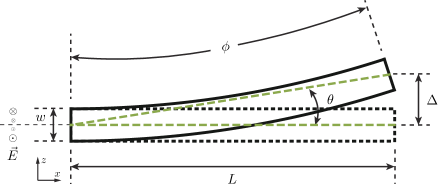
Bending of the beam can be well described by a radius and the corresponding curvature when . The contraction and expansion on the two sides of the beam are related to the bending radius as
| (2) | |||||
| (3) |
where is the component of the field, is the width of the beam and is the corresponding central angle of the deformed beam. Subtracting the two equations, we obtain
| (4) | |||||
| (5) |
The resulting deflection angle and the deflection along the direction are given by
| (6) | |||||
| (7) |
We would like to point out that the actual displacement could be either in-plane if -cut LN is chosen such that the surface of the chip is perpendicular to , or out-of-plane on -cut LN, where the surface of the chip is perpendicular to , so long as is generated by the electrode configuration. In addition, the above discussion holds for any piezoelectric material with a non-vanishing transverse piezoelectric coefficient.
More generally, the non-uniform electric field can be approximated to first order as
| (8) |
The spatially uniform component of the field is ignored. The electrodes for generating the field are assumed to have a translational symmetry along the direction of the beam (-axis), thus the component is negligible. Furthermore, the magnitude of LN’s is more than one order of magnitude larger than the other non-zero transverse piezoelectric coefficients. Therefore, we only consider the piezoelectric component and the only relevant electric field component is . The validity of this approximation is confirmed by simulations in Sec. A.2.1.
The full piezoelectric constitutive equations in the strain-charge form are
| (9) | |||||
| (10) |
where is the compliance matrix, is the unclamped permittivity, is the electric displacement and is the stress. For a nanobender anchored on one end under one volt applied voltage, the stress in the body of the beam is typically from simulation. The compliance of LN is , thus . On the other hand, the electric field while , leading to . As a consequence, Eq. 9 can be well approximated by . This observation agrees with the intuition one would have for a mostly free beam, where the internal stress is expected to be small. Larger stress is localized near the surface of the beam at the boundary of the electrodes, where the electric boundary condition is not continuous.
The displacement field can be solved from the strain field and for all other components. For a free beam with and ignoring any rigid rotation,
| (11) | |||||
| (12) |
As a result, bending of the beam is observed for both and direction, where the displacement at scales quadratically with the length of the beam . The displacement along the direction is identical to Eq. 7.
In the above derivation, and are assumed to be uniform on the cross-section of the beam. In reality for a -cut nanobender where a parallel pair of electrodes is placed on the top surface (- plane) of the beam, the fringing field has a complicated spatial variation. Nevertheless, the field mostly varies along the direction and the variation along is negligible after averaging over the cross section. Similarly, the field mostly varies along the direction. We verify this by numerically evaluating the average of on the cross section for using COMSOL simulations. The averaged and are two orders of magnitude smaller than and . This can be qualitatively understood by considering the symmetry of the electrostatic potential and the electric field. The parallel pair of electrodes possess -reflection symmetry, where the geometry of the electrodes is invariant under reflection with respect to the symmetry plane . When a voltage difference is applied to the electrodes and by setting the potential reference such that on , we have approximately . Consequently,
| (13) | |||||
| (14) | |||||
| (15) | |||||
| (16) |
The implication from these observations is that and average to roughly zero on the cross section. Intuitively speaking, by virtually dividing the beam into two halves separated by the -symmetry plane, the two halves of the beam tend to bend against each other when and are considered, thus cancelling and leading to an insignificant deformation of the full beam. In contrast, they bend in accordance with each other from or , generating a much larger bending of the full beam. Similarly for a -cut nanobender where the electrodes are fabricated on the - plane, -reflection symmetry can be considered, and the same arguments still hold.
As discussed above, the bending from Eq. 11 is mostly along a single direction , generating a “clean” displacement . In other words, for a nanobender where only is considered as non-zero and the cross-section is symmetric under or reflection, the bending generates a displacement along the direction.
For example, on a -cut LN nanobender, the displacement is mostly in-plane (out-of-plane) where displacements along the other directions are more than one order of magnitude smaller (see Sec. A.2 for simulation results). The largest contribution to displacements along the other directions is bending generated by a different transverse piezoelectric coefficient.
Lastly we would like to point out that the transverse piezoelectric coefficients (-type) are not the only components that could potentially generate bending from a non-uniform electric field. Through numerical simulation (Sec. A.2), we found that the diagonal components (-type) and the shear components (-type) are also capable of generating bending under the parallel-pair electrode configuration.
A.2 Simulation of one-volt displacement
We use the Piezoelectric Devices module in COMSOL for simulating the 3D model of the nanobender. A rotated coordinate system is adopted to account for different crystal cuts and nanobender orientations. A fixed constraint is applied to one end of the nanobender while the other surfaces are subject to a free boundary condition. The metal surfaces are selected and assigned as either ground or a voltage terminal with . The full geometry is encapsulated in air for the electrostatics simulation. We found that the air encapsulation causes only a minor effect due to LN’s large relative permittivity. A stationary study is solved for the static displacement, and an eigenfrequency study is solved for the eigenmode frequencies of the nanobender.
For generality and simplicity, from now on we adopt a global coordinate system, with axes denoted by and that are fixed with the nanobender, where is parallel to the nanobender and is pointing from the fixed-end to the free-end. Positive axis is perpendicular to the chip. We report the simulated displacements in this global coordinate system. As a result, for nanobenders parallel to crystal axis as discussed above, the bending is always towards the crystal axis. The cut of the crystal is defined as the crystal axis perpendicular to the plane of the thin film from which the beam is fashioned. Since we often put electrodes on top of the thin film, the example in the beginning of the supplementary information would naturally correspond to a -cut film where the beam is patterned to be parallel to the crystal . In the newly defined chip coordinate system, we have , , , and therefore a large displacement being generated in which is in the plane of the chip. Similarly, for -cut nanobenders, a vertical bending results and leads to a large .
A.2.1 Contributing piezoelectric components to the displacement
To show that the dominant contribution of the displacement is from the component of the piezoelectric tensor, we conduct finite element simulations with the original piezoelectric tensor and compare the results to simulations where all components of other than are set to zero.
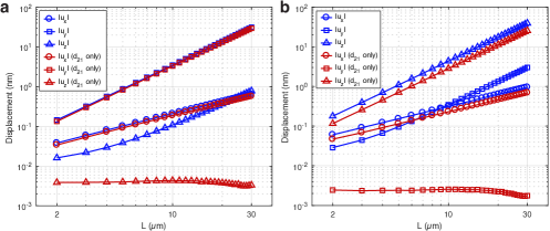
The simulated displacements are plotted in Fig. 7 for different nanobender lengths in log scale. For -cut nanobenders (Fig. 7a), the component is able to produce the simulated displacement from the full tensor with minor deviation. The quadratic scaling of versus can be clearly observed by comparing to . The large deviation between only and full simulations for can be explained by the non-zero component of LN, which generates out-of-plane bending from . Since the magnitude of is more than one order of magnitude smaller than , the vertical bending is negligible comparing to in-plane bending. However, the quadratic scaling is still present and makes larger than for sufficiently large .
As for vertical nanobenders on -cut LN, we observe (Fig. 7b) that keeping only the coefficient underestimates the full simulated displacement. The other piezoelectric components contribute to roughly of the displacement . Surprisingly we find that out of the displacement that cannot be explained by the component originates from the and components. These components are not expected to generate bending from the intuitive explanation provided in Sec. A.1, and likely result from the complicated non-uniform electric field profile.
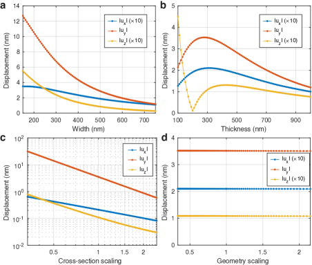
A.2.2 Dependency of displacement on nanobender geometry
So far, we have mostly considered the quadratic length-displacement relationship of the nanobender. Here, we investigate how other geometric parameters affect the displacement for both -cut and -cut nanobenders. Figures 8a and b show how the maximal displacement of the nanobender for all three directions scales with width and thickness . As expected, the displacement increases for smaller width. We also observe that for varying thickness, the in-plane displacement peaks at around nm for a fixed electrode thickness nm. Furthermore, it is interesting to see how scaling the cross-section for a fixed length affects displacement. Scaling the cross-section relative to nm, we observe (fig. 8c) that as the cross-section increases, and decrease quadratically whereas decreases linearly. Finally, following the scale-invariance argument in the main text, the displacement of the nanobender is not dependent on its relative size. By scaling the whole geometry of the nanobender relative to nm, we confirm through simulations that the displacement is indeed independent of geometry scaling.
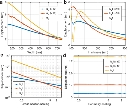
For -cut nanobenders (Fig. 9), the simulations and analysis are similar except that the out-of-plane displacement component is dominant instead of .
A.3 Approximated displacement for zigzag nanobenders
In this section, we show that the nanobender on -cut LN can be wrapped in a zigzag structure without metal crossover while maintaining efficient displacement actuation. The direction of the in-plane displacement can be controlled by the aspect ratio of the zigzag structure. Furthermore, the identical zigzag configuration generates out-of-plane deflection that accumulates along the zigzag on -cut LN.
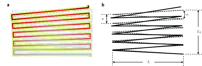
We start with a -cut zigzag nanobender. Fig. 10 shows a simulated displacement profile (Fig. 10a) and a schematic drawing of the simplified zigzag geometry (Fig. 10b). We simplify one unitcell of the zigzag structure as two solid lines which connect at the “U-turns” and form an angle . is the length of a single nanobender and is the width of one unitcell. The extension of the zigzag structure is where is the number of unit cells.
Since only the in-plane displacements are relevant, the coordinates and displacements can be represented by complex numbers. We establish a complex plane such that the real axis is parallel to a single nanobender and the origin coincides with the bottom right of the zigzag structure where it is anchored. To move along the vertices of the simplified zigzag, two complex numbers and can be added consecutively. As a result, for a zigzag nanobender with unit cells ( connected nanobenders), the position of the end point is
| (17) |
When a voltage is applied such that a single nanobender is deflected by an angle as defined in Sec. A.1, it will be shown in the following that the displacement at is solely determined by and .
As shown in Fig. 6, every nanobender in the zigzag structure contributes a rotation of from one vertex to the next vertex. Note that the rotation is instead of . One would expect if only considering the displacement. However, the next nanobender is connected tangentially to the end of the previous nanobender, which, due to the bending, has changed its orientation by . The end position of the zigzag after the series of bending and rotation can be expressed as
| (18) | |||||
The resulting displacement at the end of the zigzag is
| (19) | |||||
We have expanded the expression up to first order in , used the relationship and the approximation . Written back in vector notation, we obtain the in-plane displacement
| (20) |
where is the bending curvature that can be obtained by a single nanobender simulation, which is much faster than simulating the full zigzag structure. The total displacement is enhanced by the number of unit cells , and the direction of the displacement is related to the overall geometry of the zigzag structure and .
To compare the above simplified estimation to the simulated displacement, we evaluated the maximal displacements from three different zigzag structures using COMSOL and using the estimation Eq. 20. The comparison is shown in Table 2. A one-volt curvature of obtained from a single nanobender simulation is used. We see reasonable agreement between simulated and estimated displacements for zigzags with various aspect ratios , where the deviations are all .
| () | () | Simulated () | Estimated () | |
|---|---|---|---|---|
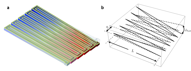
When -cut zigzag nanobenders are considered for out-of-plane actuation, the situation is simpler comparing to the -cut in-plane zigzag nanobenders. The direction of bending is disentangled with the geometry of the zigzag structure, and the rotation simply accumulates along the zigzag structure (Fig. 11).
More specifically, at the end of each unit cell of the deformed zigzag, the tangential direction is changed by . After unit cells, the accumulated angle is where is the bending curvature. For a one-volt , and , degrees. A deflection of degrees can be achieved with voltages between .
As for the corresponding vertical displacement, it is directly given by . This is much smaller than the displacement generated by a single nanobender with the same total length , which is . Since a large displacement is transduced, one expects the effective stiffness of the single nanobender with length to be much smaller than the zigzag structure. To verify this, we simulated the displacement of a zigzag nanobender with and under a vertical force of at the end of the zigzag, and also the displacement of a single nanobender with under the same conditions. The simulated displacements are for the zigzag and for the single nanobender.
From Euler-Bernoulli beam theory (see also Sec. F.1), the effective spring constant of a beam scales as . By approximating the joint between every nanobenders in the zigzag structure as a stiff connection, the effective spring constant of the zigzag is , where the proportionality coefficient is determined by material properties and the cross section geometry. On the other hand, the single nanobender has . As a result, the single nanobender is a factor of less stiff than the zigzag nanobender. Note that the central angle generated by the single nanobender is , identical to the zigzag nanobender. Hence for applications where an out-of-plane rotation is desired, the zigzag nanobender is advantageous over a single nanobender, where the zigzag nanobender generates an identical out-of-plane rotation with a much stiffer structure.
Appendix B Nanophotonic zipper cavity design and properties
B.1 Mirror cell design
In the following, we briefly describe the procedure, adapted from Ref. Jiang et al. (2019a), for designing the -cut lithium niobate mirror cell used as part of the 1D zipper nanophotonic cavity and the reflector at the end of the coupling waveguide. The thickness of the mirror cell is set to nm. Because of fabrication imperfections, the LN structures have angled sidewalls which we take into account in the design. We therefore use an outer angle (defined as the angle between the sidewall and the vertical direction) of and inner angle (inside the hole) of , based on scanning electron micrographs. The mirror cell geometry (Fig. 12a) consists of two identical halves separated by a gap . Each half is constructed by adding a cosine edge with amplitude to a rectangle with dimensions by . Half of an ellipse (with axes and ) is then cut out of the rectangle to generate an air-hole. By periodically continuing the unit cell with lattice spacing , we can open a quasi-TE optical bandgap at the -point (see Fig. 12b). Based on eigenfrequency simulations and optimization of the bandgap size, we choose the parameters nm leading to a quasi-bandgap of THz centered at THz. We used multivariable genetic optimization to determine the parameters for this geometry. The cost function tries to maximize the size of the quasi-TE bandgap at the -point while trying to push up the fundamental quasi-TM mode out of the bandgap to avoid scattering into it. The gap is set to nm.
B.2 1D nanophotonic cavity
To localize an optical mode inside a 1D nanophotonic cavity, it is standard to introduce a defect unit cell inside an array of mirror cells with a smooth set of transition cells in between. This defect cell has a fundamental quasi-TE mode at the -point that is inside the bandgap of the mirror cell. To generate the defect cell starting from the mirror cell, it is thus necessary to push up the fundamental quasi-TE mode of the mirror cell. This is achieved by reducing its lattice spacing as well as the relative air-hole size. The defect and mirror cells are smoothly connected through cubic interpolation Chan (2012) using transition cells (see Fig. 12c). We additionally have mirror cells on each side of the cavity.
We determine the geometry of the defect cell with a similar multivariable genetic optimization. The cost function maximizes the optical quality factor of the localized fundamental optical mode while disregarding solutions that lead to unphysically high s Jiang et al. (2019a). As a result of this optimization, a defect cell geometry with parameters nm is chosen, and the number of transition cells and mirror cells are determined to be and respectively. Fig. 12d shows the simulated fundamental quasi-TE mode profile for this design choice. Furthermore, we see that the resonance wavelength of the cavity is strongly dependent on the gap of the cavity (Fig. 12e) leading to a large optomechanical coupling for the fundamental in-plane mechanical mode of the bender-zipper structure.
Appendix C Optical background removal
In this section, we describe how we remove wavelength-dependent background fluctuations in optical reflection measurements that involve DC tuning. These fluctuations arise in the measurement setup and are not part of the actual device response. An example of raw DC tuning measurement data is shown in figure 13a. Even though it is still possible to see tuning of the mode, the background makes it difficult to process the data. Additionally, modes that are very weakly coupled can be hidden by the background. To remove the fluctuations in the background we use the fact that the resonance wavelength of the mode tunes with voltage whereas the background is static. For each wavelength, we can thus take the mean of the reflection over the DC voltages. Formally, for a reflection at wavelength and voltage , we compute the mean where is the number of voltages. We then normalize the reflection and recover the plot shown in Fig. 13b. The fluctuating background is removed whereas the tunable modes are not affected. In Fig. 13 we show a comparison of the raw and normalized reflection spectrum at V and see that the normalized background is flat. Because the control optical mode is static, we expect it to be removed through normalization. However, it is still visible, although slightly distorted. By looking at the control mode more carefully, we observe that it is slightly drifting with time as the experiment is being carried on, which means it is not perfectly static. Looking at a close up of one of the tunable modes (Fig. 13d), we see that neither the wavelength nor the linewidth of the mode are affected by the background removal.
Appendix D Low temperature and pressure measurements
D.1 Thermal broadening
In this section, we show that the optical linewidths of the bender-zipper cavities are limited by thermal-mechanical broadening at room temperature. This effect causes the Lorentzian lineshape of the resonance to be convoluted by a Gaussian distribution representing the random position of the mechanical degree of freedom due to Brownian motion. The resulting profile is the so-called Voigt profile Winger et al. (2011). If the linewidth of the Gaussian is much larger than the linewidth of the cavity resonance , then the linewidth of the Voigt profile is
| (21) |
To compute this broadened linewidth , we proceed with calculating the root mean square displacement caused by thermal Brownian motion. We consider one half of a bender-zipper cavity. By simulating the displacement profile of the fundamental mechanical in-plane mode, we calculate the effective motional mass associated with it through Chan (2012):
Here, is the density of the material and u(x) is the displacement field. This mechanical mode has a frequency MHz. Using the equipartition theorem, we find Winger et al. (2011):
Here, K is the room temperature and is the Boltzmann constant. The root mean square displacement of the full bender-zipper cavity is then simply given by: pm. From optical resonance wavelength versus zipper cavity gap size simulations (Fig. 12e), we extract the optomechanical coupling GHz/nm. This value assumes a gap size of nm. Finally, the broadened linewidth is given by Winger et al. (2011):
At a temperature of K, the same expression leads to pm. We therefore expect the linewidth of the cavity to decrease at low temperatures if it is limited by thermal broadening.
In Fig. 14 we compare the measured reflection spectrum of a tunable bender-zipper cavity at room temperature and in a K cryostat. We observe that the linewidth decreases from pm to pm when cooling down which is more than an order of magnitude. The room temperature linewidth is on the same order as the theoretically predicted broadening. Because the gap is difficult to accurately measure, so is estimating . This could help explain the difference between predicted and measured values for the broadened linewidth. Additionally, simulating the full bender-zipper cavity as well as taking into account more mechanical modes that lead to broadening could help compute a more accurate value for the linewidth. In the low temperature case, is comparable to and so equation 21 does not hold anymore. Moreover, the resonance wavelength gets blue-shifted from nm to nm when cooling down which is expected from thermal contraction and refractive index change. The measured bender-zipper cavity has a gap nm which we extract from a scanning electron micrograph taken before release. The device was cooled down using a closed-cycle Montana Instruments cryostat.
Finally, we compute the zero-point fluctuation for the full bender-zipper cavity which is given by Chan (2012):
This allows us to obtain the vacuum optomechanical coupling strength MHz.
D.2 Mechanical quality factor as a function of pressure
We investigate how the thermal-mechanical power spectrum of the bender-zipper cavity changes when pressure is decreased. At atmospheric pressures, the mechanical quality factor is limited by air damping. We use the cryostat from the previous section as a vacuum chamber at room temperature and measure the thermal-mechanical spectrum as the chamber is being pumped down. We extract as a function of pressure (Fig. 14b and 14c). As the pressure decreases, the quality factor increases at a slightly sub-linear rate. We observe a two-order of magnitude increase in the mechanical quality factor, reaching at mbar. Extrapolating this rate to atmospheric pressure at mbar agrees well with measurement. Below mbar, we can see start saturating, showing that air damping is no longer the main mechanism for dissipation. Thermo-elastic damping starts becoming dominant at room temperature and low pressure, so we expect to further improve at low temperature.
Appendix E Rotated nanobenders
We have considered -cut LN where the nanobender is parallel to the crystal axis. In this section we investigate how changing the in-plane orientation of the nanobender affects the displacement of the nanobender. This amounts to changing the angle between and (parallel to the nanobender), where is the crystal axis, is the global coordinate fixed with the nanobender and is pointing from the fixed-end towards the free-end of the nanobender. Global axis is perpendicular to the chip (parallel to crystal axis).
A good indicator for how the displacement varies with is to look at how the rotated piezoelectric components and change with (Fig. 15a). As discussed in Sec. A.1, () couples between () and , and generates vertical (horizontal) bending from (). We can directly compare it to simulated displacements of a nanobender with where is swept from to .
Plotting the maximal and minimal value of the displacement (Fig. 15b), we see that the out-of plane component varies approximately as . The in-plane displacement component perpendicular to the nanobender follows relatively well when is changed, although the resulting curves are asymmetric. We attribute this to one end of the nanobender being anchored, breaking the symmetry, and also contributions from other non-zero piezoelectric components. When , we see that the in-plane displacement is reduced by a factor . Moreover, for a bender-zipper cavity, two nanobenders rotated by are attached to the two ends of the same half of the zipper cavity. The two nanobenders would bend towards opposite directions (Fig. 15b, at and ) if they were not connected, leading to a small net displacement. From simulations of a rotated bender-zipper cavity, we find that decreases by more than one order of magnitude.
We fabricate and measure such a bender-zipper cavity where . The device (Fig. 15c) does not have a waveguide with a bend as opposed to the bender-zipper cavity aligned along crystal axis in the main text. Moreover the nanobenders are attached to the zipper cavity through small tethers. We confirm that the active bender-zipper cavity is free to move by measuring its thermal-mechanical power spectral density (Fig. 15d) which looks typical of previously measured tunable devices. As expected, the DC tuning measurement of the rotated device (Fig. 15e and f) shows only little tuning. We extract a DC tuning coefficient of nm/V which is significantly smaller than devices with where we measure nm/V. Moreover, we measure that the control zipper cavity does not tune at all.
Lastly it is worth noting that according to the simulation results, a variety of actuation directions can be achieved with the same crystal cut by fabricating the nanobender along different in-plane orientations. For example, relatively clean vertical actuation can be achieved at degrees even on -cut LN.
Appendix F Mechanical mode frequency and AC modulation measurement
F.1 Fundamental mechanical mode frequency as a function of nanobender length
In this section, we study the actuation speed of a single nanobender as well as the tuning speed of the bender-zipper cavity. For the case of a single nanobender, Euler-Bernoulli beam theory allows us to write a simple expression for its fundamental eigenfrequency. The in-plane fundamental eigenfrequency of a beam clamped on one side, is given by Cleland (2013)
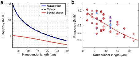
where is Young’s modulus, is the second moment of area and is the mass per unit length. The density of LN is . The agreement with finite element method simulations (see Fig. 16a) is very good, overestimating the actual values by only . This deviation arises because the analytical expression is not taking into account the anisotropy of LN (we approximated LN as an isotropic material and took Pa Weis and Gaylord (1985)). Furthermore, the analytical expression does not include the aluminum electrodes which would decrease the frequency due to the much smaller Young’s modulus of aluminum. We can recover the spring constant of the nanobender: N/m for . This lets us convert the displacement actuation to an equivalent force per volt of . Because scales as and scales as , the force per volt scales as .
In Fig. 16a, we also show the simulated fundamental resonance frequency of one half of a bender-zipper cavity as a function of the nanobender length . As expected, for small , the nanobender is not limiting the tuning speed of the cavity but rather the size of the cavity itself. In Fig. 16b, we compare this simulated curve to experimental values obtained from thermal mechanical spectra of bender-zipper cavities. For each device, we observe multiple resonance frequencies which are spread around the curve obtained from simulation. Simulating the full structure should lead to a splitting of the resonance frequency due to the mechanical coupling between the two identical halves of the bender-zipper cavity.
F.2 AC wavelength shift as a function of modulation voltage
Here, we experimentally confirm that the AC wavelength shift of the bender-zipper cavity is linear with respect to the driving voltage . In Fig. 17a, we show results of modulation experiments where we sweep from to mV. This measurement is done for two different resonance frequencies of the bender-zipper cavity (see Fig. 3e in the main text). We proceed as in the main text and extract as a function of by doing an analytical fit and converting bias voltage to wavelength. These are plotted in Fig. 17b. By fitting a line, we extract the AC tuning coefficient for a specific resonance frequency. We find that the AC tuning coefficient is independent of for the range of voltages considered here, validating the voltage normalization done in Fig. 3e of the main text.