Designing Few-layer Graphene Schottky Contact Solar Cell: Theoretical Efficiency Limits and Parametric Optimization
Abstract
We theoretically study the efficiency limits and performance characteristics of few-layer graphene-semiconductor solar cells (FGSCs) based on a Schottky contact device structure. We model and compare the energy conversion efficiency of various configurations by explicitly considering the non-Richardson thermionic emission across few-layer graphene/semiconductor Schottky heterostructures. The calculations reveal that ABA-stacked trilayer graphene-silicon solar cell exhibits a maximal conversion efficiency exceeding 28% due to a lower reversed saturation current when compared to that of the ABC-stacking configuration. The thermal coefficients of PCE for ABA and ABC stacking FGSCs are -0.064%/K and -0.049%/K, respectively. Our work offers insights for optimal designs of graphene-based solar cells, thus paving a route towards the design of high-performance FGSC for future nanoscale energy converters.
Two-dimensional-material-based heterostructures have been actively explored Akinwande, Petrone, and Hone (2014); Fiori et al. (2014); Wang and Xia (2015); Rodriguez-Nieva, Dresselhaus, and Song (2016) in recent years due to their widespread applications in nanoelectronics, nanophotonics, and optoelectronics, such as energy harvesting Li et al. (2010); Javadi (2020); Zhang et al. (2018), transistors Wang et al. (2019); Choi et al. (2019); Jiang et al. (2020), photo detection Lopez-Sanchez et al. (2013), sensors Kim et al. (2013), and data storage devicesLi et al. (2017). Due to their unusual optical and electronic properties, 2D materials have immense potential for next-generation solar cells Das et al. (2019); Cheng et al. (2018). With the scaling trends in photovoltaics moving toward thin, atomically-thin 2D materials with high mechanical strength and flexibility have become the key candidate materials for the development of next-generation photovoltaic technology. In terms of solar energy harvesting, 2D-metal/3D-semiconductor solar cells, especially graphene-silicon contact, have been extensively studied Li, Lv, and Zhu (2015); Won (2010); Ihm et al. (2010); Li et al. (2014), with a particularly strong emphasis on improving the power generation efficiency of the device Miao et al. (2012); Shi et al. (2013); Meng et al. (2016). The record PCE of such devices has been rising steadily in recent years, achieving an exceptional values of 15.6% and 18.5%, respectively, for graphene/silicon Song et al. (2015) and graphene/GaAs Li et al. (2015) solar cells.
Despite extensive research focusing on monolayer graphene solar cells, few-layer-graphene/semiconductor solar cells (FGSCs) with a new transport mechanism remain relatively less explored. Correspondingly, the fundamental efficiency limit and performance characterization of FGSCs remain poorly understood. Importantly, FLG is known to possess completely different electrical and optical properties when compared to monolayer graphene Nakamura and Hirasawa (2008); Zhu, Yuan, and Janssen (2014); Mak et al. (2010). The incorporation of FLG with 3D semiconductors has thus led to myriads of interfacial transport and charge injection phenomena that are distinctive from the monolayer counterpart Ang and Ang (2016); Sinha and Lee (2014); Ang, Yang, and Ang (2018); Trushin (2018); Javadi et al. (2019). In relevance to solar cell applications, employing FLG as a top-layer material offers the following advantages. Firstly, FLG possesses high transparency in the visible range of the solar spectrum, thus ensuring sunlight transmission into the semiconductor medium with small enough optical loss. Secondly, FLG exhibits a lower reverse saturation current in contrast to conventional metal and monolayer graphene. As the layer number increases, the series resistance and ideality factor in FLG-based Schottky devices are vanishingly small. Thirdly, since the depletion region forms on the right side of the semiconductor surface, FGSCs are characterized by high photocurrent generation and considerable short-wavelength photoresponse. Benefited by these factors, FGSCs hold strong potential as a candidate materials for low-cost and high-efficiency solar-to-electricity energy conversion.
In this Letter, we investigate the various performance metrics and efficiency limits of FGSCs (see Fig. 1) by harnessing the thermionic emission process in FLG-semiconductor Schottky junctions. Here we consider two forms of FLG: ABA and ABC stacking order configurations, which exhibits layer-and stacking-dependent electronic band structures. To gain physical insights into the main limiting factors and further improve the device performance, we perform a computational study to understand how the device performance are influenced by the effect of stacking order, semiconductor bandgap, layer number of FLG, and temperature. Our results offer practical insights on the optimum design of high-performance FGSCs, thus offering an important theoretical basis for the exploration of 2D-material-based solar energy harvesting technology.
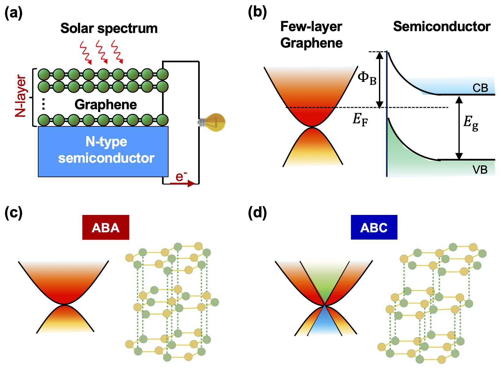
We model an ideal FGSC and determine its theoretical efficiency limit based on the following assumptions: (i) Each incident photon with energy higher than the semiconductor bandgap [ in Fig. 1(b)] can produce an electron–hole pair that contribute to the photocurrent, i.e., negligible recombination of excess carriers. (ii) The device ideality factor is , and ohmic loss due to the series resistance is expected to be small. Such ideal conditions may be approached practically via FLG because both the series resistance and ideality factor are shown to decrease with the number of graphene layers Jie, Zheng, and Hao (2013). The characteristic of the 2D-material/semiconductor Schottky contact at room temperature exhibits a rectifying behavior as governed by the Shockley diode equation,
| (1) |
where represents the short circuit photocurrent density, denotes the reversed saturation current density (RSCD) due to thermionic emission over the Schottky barrier [, see Fig. 1(b)] under a bias voltage , is the electron charge, is the Boltzmann constant, and is the operating temperature of the cell. The short-circuit current or photocurrent density generated by sunlight absorption in FSSC is
| (2) |
where is the incident photon flux of AM1.5D terrestril solar spectrum with wavelength range of 280 nm to 4000 nm. Here represents the optical transmittance of FLG, which can be obtained from experimental data Zhu, Yuan, and Janssen (2014); Mak et al. (2010). is the bandgap of the semiconductor, and represents the photon energy with frequency . The open-circuit voltage can then be obtained as
| (3) |
For an ideal Schottky contact, the transport of charge carriers is governed by the thermionic emission over the Schottky barrier at the contact interface and the corresponding RSCD is given by a generalized thermionic emission model
| (4) |
where the prefactor and the scaling exponent are material-and interface-dependent parameters Ang, Yang, and Ang (2018). The scaling exponent takes the form of and A/cm2K for a classic Schottky contact composed of 3D bulk metals with parabolic energy dispersion. For FLG-based vertical Schottky contact, the electronic properties of the FLG Ang and Ang (2016); Sinha and Lee (2014); Ang, Yang, and Ang (2018); Trushin (2018); Javadi et al. (2019), deviates significantly from the parabolic energy dispersion. Furthermore, the electronic properties of FLG exhibit nontrivial dependences on the number of layers and the layer stacking order. For instance, the bernal (i.e. the ABA stacking order) and the rhombohedral (i.e. the ABC stacking order) FLG – the most thermodynamically stable stacking orders Neto et al. (2009) [see Fig. 1(c) and (d)] – display highly nonparabolic energy dispersions. Such band structure nonparabolicity gives rise to an unconventional and non-Richardson RSCD whose temperature scaling behavior is drastically different from that of the classic Richardson thermionic emission model. In this case, the vertical FLG-semiconductor Schottky heterostructures obeys a current-temperature scaling exponent of , with the following layer number and stacking order dependent prefactor Ang, Yang, and Ang (2018):
| (5) |
where represents the FLG layer number, is a charge injection characteristic time constant whose value is influenced by the quality of the contact, is the reduced Plack’s constant, and m/s. Here, the RSCD shows an -fold enhancement in ABA FLG due to the presence of conduction subbands. This is in stark contrast to ABC FLG where the RSCD has a nonlinear -dependent prefactor.
The PCE of the FGSC is defined as the ratio of the maximum electric power to the total incoming solar photon energy flux , i.e.
| (6) |
where is the fill factor. The maximum power point can be determined by solving .
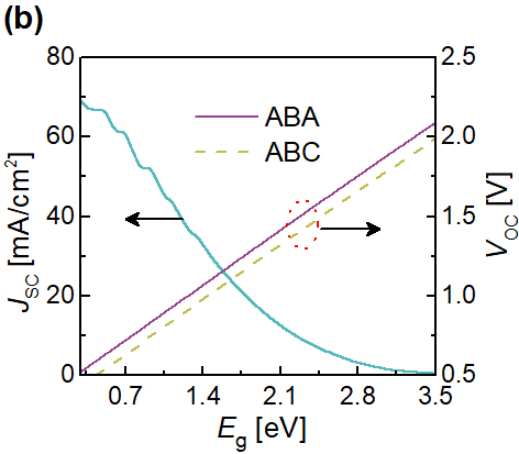
For a given semiconductor, the PCE increases with the Schottky barrier height as indicated in Eq. (4). Taking the semiconductor bandgap as the ultimate boundary of the Schottky barrier height, i.e., , we obtain the upper limits of the PCE for the FGSC. We choose a relatively larger injection time of ps to represent the inevitable presence of defects at the Schottky contact interface. Figure 2(a) shows the PCE of the FGSC as a function of the semiconductor bandgap at room temperature. The small oscillations originate from the atmospheric absorption in the incident AM1.5D solar spectrum. The efficiency bounds of the FGSC reveal a broad range from 0.8 to 1.5 eV with PCE exceeding 25%. For narrow-bandgap semiconductors, although a high photocurrent density is warranted, the output voltage remains low due to the limited Schottky barrier height (or bandgap) as expected from Eq. (3). On the other hand, for wide-bandgap semiconductors, the photon absorption is significantly impeded by the larger bandgap, which leads to a low photocurrent density [see Fig. 2(b) and Eq. (2)]. The interplay between these two counteracting behaviors leads to an optimal semiconductor bandgap for achieving maximum PEC. The open-circuit voltage is associated with , and is thus sensitively influenced by the staking order. Importantly, the open-circuit voltage of the ABA-trilayer FGSC is higher than that of the ABC FGSC. The stacking order dependence becomes particularly more pronounced at the wide-bandgap regime and causes an enhancement of the fill factor.
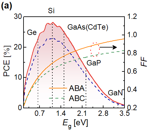
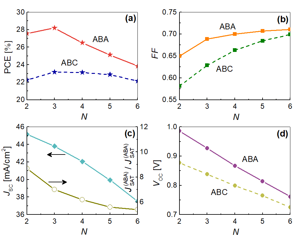
As shown in Fig. 2(a), the theoretical upper limit of the PCE for the FGSC with ABA trilayer graphene is predicted to be 28.2% at eV – a value which is very close to the bandgap of silicon. To explain why ABA stacking order reflects better performance than ABC, we choose the trilayer graphene/Si solar cell as an illustrative example and further access its characteristics under different operating conditions (see Fig. 3). We show that the open-circuit voltage of ABA FGSCs (0.927 V) is higher than that of ABC FGSCs (0.838 eV), although both of them exhibit the same short-circuit current density of 43.8 mA/cm2. These facts demonstrate the key advantage of the ABA-stacking order in achieving high-performance Schottky-contact based solar energy converter. It is worth mentioning that the classic Richardson thermionic emission model, which does not accurately capture the reduced dimensionality and the nonparabolic nature of the energy dispersion in FLG, can yield a discrepancy in the thermionic current density of about 2 orders of magnitude Ang and Ang (2016). In relevance to the modeling of FGSC, using the classic Richardson model of A/cm2 K2 and can lead to an overly small open-circuit voltage as well as a low PCE ( V and PCE=18.6%). This finding highlights the importance of utilizing the appropriate thermionic emission that better captures the material properties of FLG during the modeling of Schottky-contact based energy converters.
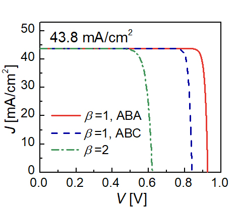
Figure 4(a-d) shows the PEC, fill factor, short-circuit current density, and open-circuit voltage of the ABA and ABC FGSC as a function of the layer number of graphene. We consider because the work function of FLG with more than 6 layers tends to saturate at that of graphite. We identify an optimal layer number of that yields the maximum PCE. When the layer number is increased from to , the fill factor incraeses substantially. However, as the layer number is further increased, the FF becomes saturated [Fig. 4(b)]. In contrast, the short-circuit current density and the open-circuit voltage exhibit a monotonous decreasing trend with the layer number Fig. 4(c) [Fig. 4(d)]. The trade-off between the fill factor, short-circuit current density, and the open-circuit voltage leads to an optimal layer number maximizing the PCE. To compare the RSCD of FLG with ABA and ABC stacking, we define the ratio of and plot the layer dependence of this ratio in Fig. 4(c). The is about an order of magnitude larger than , which reveals the fundamental origin of the better ABA FGSC performance in providing a larger open-circuit voltage and a higher PCE when compared to that of the ABC FGSC.
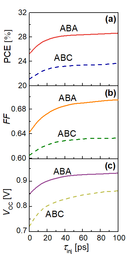
We further study the -dependence of the PCE, fill factor, and the open-circuit voltage in Figs. 5(a-c). The is related to the contact quality between the FLG and the semiconductor. Here we consider a representative range from 0.1 ps to 100 ps, which is consistent with the values reported experimentally Sinha and Lee (2014); Xia et al. (2011); Massicotte et al. (2016); Trushin (2018). A larger corresponds to the situation in which the contact resistance across the Schottky contact is large Sinha and Lee (2014). In general, the key performance parameters of the FGSC is influenced by the values of . Particularly when is small, increasing leads to a significant improvement of the PCE, fill factor, and the open-circuit voltage [see Fig. 5(a-c)]. Such improvement eventually saturates as is further increased. This analysis thus suggests that electrical contact engineering may offer a route to improve the system performance of FGSCs.
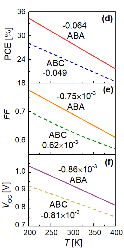
Since the RSCD is exponentially dependent on the temperature, the performance of FGSC exhibits a strong temperature dependence as shown in Fig. 5(d-f). A high operating temperatures decrease the fill factor [Fig. 5(e)] and open-circuit voltage [Fig. 5(f)], which eventually degrade the PCE [Fig. 5(d)]. Reducing the operating temperature is thus crucially important to achieve optimal energy conversion efficiency. For the ABA FGSC, the upper limit of the PCE increases (decreases) from 28.2% at room temperature to 34.4% (21.6%) at (400) K. Similarly, the maximum PCE of the ABC solar cell increases (decreases) from 23.1% at room temperature to 28.4% (18.7%) at (400) K. For both stacking orders, the efficiency limit of the FGSC acts as a nearly perfect linear function of the operating temperature, thus allowing us to define a thermal coefficient of the PCE as . For ABA trilayer graphene/silicon solar cells, we obtain %/K, signifying a drop of % in the PCE when the temperature is increased by 1 K. In the case of ABC, the thermal coefficient of PCE is found to be %/K. In addition, we also obtain the thermal coefficient of the fill factor and open-circuit voltage, as depicted in Fig. 5(e) and Fig. 5(f).
In summary, we have performed a computational modeling on the design of FGSC for solar energy harvesting. The FGSC with ABA trilayer graphene/silicon architectures possess a peak efficiency of 28.2% at room temperature, which is significantly higher than that of ABC-FLG-based devices. The better performance of ABA FLG in FGSC application originates from the lower RSCD. Importantly, an optimal layer number of is predicted. Our analysis further reveal an intriguing figure of merits, i.e. the thermal coefficient of the PCE, which allows the temperature dependence of the energy conversion performance to be accessed. Our findings shall provide practical insights useful for the design of high-performance FGSCs, thus paving a potential new avenue towards 2D-material-based solar energy harvesting technology approaching the Shockley–Queisser limit.
This project is supported by the National Science Foundation through grant number 11811530052. YSA acknowledge the supports of Singapore MOE Tier 2 Grant (2018-T2-1-007).
data availability
The data that support the findings of this study are available from the corresponding author upon reasonable request.
References
- Akinwande, Petrone, and Hone (2014) D. Akinwande, N. Petrone, and J. Hone, “Two-dimensional flexible nanoelectronics,” Nat. Commun. 5, 1–12 (2014).
- Fiori et al. (2014) G. Fiori, F. Bonaccorso, G. Iannaccone, T. Palacios, D. Neumaier, A. Seabaugh, S. K. Banerjee, and L. Colombo, “Electronics based on two-dimensional materials,” Nat. Nanotechnol. 9, 768–779 (2014).
- Wang and Xia (2015) X. Wang and F. Xia, “Van der waals heterostructures: Stacked 2d materials shed light,” Nat. Mater. 14, 264–265 (2015).
- Rodriguez-Nieva, Dresselhaus, and Song (2016) J. F. Rodriguez-Nieva, M. S. Dresselhaus, and J. C. Song, “Enhanced thermionic-dominated photoresponse in graphene schottky junctions,” Nano Lett. 16, 6036–6041 (2016).
- Li et al. (2010) X. Li, H. Zhu, K. Wang, A. Cao, J. Wei, C. Li, Y. Jia, Z. Li, X. Li, and D. Wu, “Graphene-on-silicon schottky junction solar cells,” Adv. Mater. 22, 2743–2748 (2010).
- Javadi (2020) M. Javadi, “Theoretical efficiency limit of graphene-semiconductor solar cells,” Appl. Phys. Lett. 117, 053902 (2020).
- Zhang et al. (2018) X. Zhang, Y. Zhang, Z. Ye, W. Li, T. Liao, and J. Chen, “Graphene-based thermionic solar cells,” IEEE Electron Device Lett. 39, 383–385 (2018).
- Wang et al. (2019) Y. Wang, J. Zhang, G. Liang, Y. Shi, Y. Zhang, Z. R. Kudrynskyi, Z. D. Kovalyuk, A. Patanè, Q. Xin, and A. Song, “Schottky-barrier thin-film transistors based on hfo2-capped inse,” Appl. Phys. Lett. 115, 033502 (2019).
- Choi et al. (2019) W. Choi, D. Yin, S. Choo, S.-H. Jeong, H.-J. Kwon, Y. Yoon, and S. Kim, “Low-temperature behaviors of multilayer mos2 transistors with ohmic and schottky contacts,” Appl. Phys. Lett. 115, 033501 (2019).
- Jiang et al. (2020) B. Jiang, H. Huang, R. Chen, G. Li, D. Flandre, D. Wan, X. Chen, X. Liu, C. Ye, and L. Liao, “Black phosphorus field effect transistors stable in harsh conditions via surface engineering,” Appl. Phys. Lett. 117, 111602 (2020).
- Lopez-Sanchez et al. (2013) O. Lopez-Sanchez, D. Lembke, M. Kayci, A. Radenovic, and A. Kis, “Ultrasensitive photodetectors based on monolayer mos2,” Nat. Nanotechnol. 8, 497–501 (2013).
- Kim et al. (2013) H.-Y. Kim, K. Lee, N. McEvoy, C. Yim, and G. S. Duesberg, “Chemically modulated graphene diodes,” Nano Lett. 13, 2182–2188 (2013).
- Li et al. (2017) D. Li, M. Chen, Q. Zong, and Z. Zhang, “Floating-gate manipulated graphene-black phosphorus heterojunction for nonvolatile ambipolar schottky junction memories, memory inverter circuits, and logic rectifiers,” Nano Lett. 17, 6353–6359 (2017).
- Das et al. (2019) S. Das, D. Pandey, J. Thomas, and T. Roy, “The role of graphene and other 2d materials in solar photovoltaics,” Adv. Mater. 31, 1802722 (2019).
- Cheng et al. (2018) K. Cheng, Y. Guo, N. Han, X. Jiang, J. Zhang, R. Ahuja, Y. Su, and J. Zhao, “2d lateral heterostructures of group-iii monochalcogenide: Potential photovoltaic applications,” Appl. Phys. Lett. 112, 143902 (2018).
- Li, Lv, and Zhu (2015) X. Li, Z. Lv, and H. Zhu, “Carbon/silicon heterojunction solar cells: state of the art and prospects,” Adv. Mater. 27, 6549–6574 (2015).
- Won (2010) R. Won, “Photovoltaics: Graphene–silicon solar cells,” Nat. Photonics 4, 411 (2010).
- Ihm et al. (2010) K. Ihm, J. T. Lim, K.-J. Lee, J. W. Kwon, T.-H. Kang, S. Chung, S. Bae, J. H. Kim, B. H. Hong, and G. Y. Yeom, “Number of graphene layers as a modulator of the open-circuit voltage of graphene-based solar cell,” Appl. Phys. Lett. 97, 032113 (2010).
- Li et al. (2014) Y. Li, W. Yang, Z. Tu, Z. Liu, F. Yang, L. Zhang, and R. Hatakeyama, “Schottky junction solar cells based on graphene with different numbers of layers,” Appl. Phys. Lett. 104, 043903 (2014).
- Miao et al. (2012) X. Miao, S. Tongay, M. K. Petterson, K. Berke, A. G. Rinzler, B. R. Appleton, and A. F. Hebard, “High efficiency graphene solar cells by chemical doping,” Nano Lett. 12, 2745–2750 (2012).
- Shi et al. (2013) E. Shi, H. Li, L. Yang, L. Zhang, Z. Li, P. Li, Y. Shang, S. Wu, X. Li, J. Wei, et al., “Colloidal antireflection coating improves graphene–silicon solar cells,” Nano Lett. 13, 1776–1781 (2013).
- Meng et al. (2016) J.-H. Meng, X. Liu, X.-W. Zhang, Y. Zhang, H.-L. Wang, Z.-G. Yin, Y.-Z. Zhang, H. Liu, J.-B. You, and H. Yan, “Interface engineering for highly efficient graphene-on-silicon schottky junction solar cells by introducing a hexagonal boron nitride interlayer,” Nano Energy 28, 44–50 (2016).
- Song et al. (2015) Y. Song, X. Li, C. Mackin, X. Zhang, W. Fang, T. Palacios, H. Zhu, and J. Kong, “Role of interfacial oxide in high-efficiency graphene–silicon schottky barrier solar cells,” Nano Lett. 15, 2104–2110 (2015).
- Li et al. (2015) X. Li, W. Chen, S. Zhang, Z. Wu, P. Wang, Z. Xu, H. Chen, W. Yin, H. Zhong, and S. Lin, “18.5% efficient graphene/gaas van der waals heterostructure solar cell,” Nano Energy 16, 310–319 (2015).
- Nakamura and Hirasawa (2008) M. Nakamura and L. Hirasawa, “Electric transport and magnetic properties in multilayer graphene,” Phys. Rev. B 77, 045429 (2008).
- Zhu, Yuan, and Janssen (2014) S.-E. Zhu, S. Yuan, and G. Janssen, “Optical transmittance of multilayer graphene,” EPL (Europhysics Letters) 108, 17007 (2014).
- Mak et al. (2010) K. F. Mak, M. Y. Sfeir, J. A. Misewich, and T. F. Heinz, “The evolution of electronic structure in few-layer graphene revealed by optical spectroscopy,” Proc. Natl. Acad. Sci. USA 107, 14999–15004 (2010).
- Ang and Ang (2016) Y. Ang and L. Ang, “Current-temperature scaling for a schottky interface with nonparabolic energy dispersion,” Phys. Rev. Appl. 6, 034013 (2016).
- Sinha and Lee (2014) D. Sinha and J. U. Lee, “Ideal graphene/silicon schottky junction diodes,” Nano Lett. 14, 4660–4664 (2014).
- Ang, Yang, and Ang (2018) Y. S. Ang, H. Y. Yang, and L. Ang, “Universal scaling laws in schottky heterostructures based on two-dimensional materials,” Phys. Rev. Lett. 121, 056802 (2018).
- Trushin (2018) M. Trushin, “Theory of thermionic emission from a two-dimensional conductor and its application to a graphene-semiconductor schottky junction,” Appl. Phys. Lett. 112, 171109 (2018).
- Javadi et al. (2019) M. Javadi, A. Noroozi, A. Mazaheri, and Y. Abdi, “Sequentially assembled graphene layers on silicon, the role of uncertainty principles in graphene–silicon schottky junctions,” Adv. Opt. Mater. 7, 1900470 (2019).
- Jie, Zheng, and Hao (2013) W. Jie, F. Zheng, and J. Hao, “Graphene/gallium arsenide-based schottky junction solar cells,” Appl. Phys. Lett. 103, 233111 (2013).
- Neto et al. (2009) A. C. Neto, F. Guinea, N. M. Peres, K. S. Novoselov, and A. K. Geim, “The electronic properties of graphene,” Rev. Mod. Phys. 81, 109 (2009).
- Xia et al. (2011) F. Xia, V. Perebeinos, Y.-m. Lin, Y. Wu, and P. Avouris, “The origins and limits of metal–graphene junction resistance,” Nat. Nanotechnol. 6, 179–184 (2011).
- Massicotte et al. (2016) M. Massicotte, P. Schmidt, F. Vialla, K. Watanabe, T. Taniguchi, K.-J. Tielrooij, and F. H. Koppens, “Photo-thermionic effect in vertical graphene heterostructures,” Nat. Commun. 7, 1–7 (2016).