Topological Graphene plasmons in a plasmonic realization of the Su-Schrieffer-Heeger Model
Abstract
Graphene hybrids, made of thin insulators, graphene, and metals can support propagating acoustic plasmons (AGPs). The metal screening modifies the dispersion relation of usual graphene plasmons leading to slowly propagating plasmons, with record confinement of electromagnetic radiation. Here, we show that a graphene monolayer, covered by a thin dielectric material and an array of metallic nanorods can be used as a robust platform to emulate the Su-Schrieffer-Heeger model. We calculate the Zak’s phase of the different plasmonic bands to characterise their topology. The system shows bulk-edge correspondence: strongly localized interface states are generated in the domain walls separating arrays in different topological phases. We find signatures of the nontrivial phase which can directly be probed by far-field mid-IR radiation, hence allowing a direct experimental confirmation of graphene topological plasmons. The robust field enhancement, highly localized nature of the interface states, and their gate-tuned frequencies expand the capabilities of AGP-based devices.
Topology can lead to intriguing physical phenomena and it is at the heart of modern condensed matter physics Hasan and Kane (2010); Qi and Zhang (2011); Ren et al. (2016); Wang and Zhang (2017). It has been successfully extended to various classical wave systems, such as photonics Lu et al. (2014); Ozawa et al. (2019); Silveirinha (2015), acoustic Yang et al. (2015) and mechanical systems Ma et al. (2019). It also has been playing an increasingly important role in nanophotononics Rider et al. (2019), offering alternative ways to design novel optical devices Ota et al. (2020).
In one dimension, the celebrated Su-Schrieffer-Heeger (SSH) is probably the simplest and most representative model with non-trivial topology Su et al. (1979, 1980). Originally, it describes electrons in a one-dimensional tight-binding model with staggered hopping amplitudes, defined as intracell and intercell hoppings Su et al. (1979). Depending of the ratio between the two hopping amplitudes, the chain can have two topologically distinct ground states. The variation of this ratio leads to a topological phase transition between the two phases, with the band gap closing and reopening. If the intercell hopping is stronger than the intracell hopping, the system is in a non-trivial topological phase. In this case, the bulk-edge correspondence Rhim et al. (2017) predicts the existence of end-states, and interface states when two lattices with different topological phases are connected Heeger et al. (1988).
Photonic and plasmonic systems provide a flexible platform for the SSH model Xiao et al. (2014); Gao et al. (2015); Wang et al. (2016); Henriques et al. (2020). The effective intracell and intercell hoppings can be controlled, for example, by tuning distances via nanofabrication. Nontrivial topology in coupled plasmonic nanoparticle arrays has been previously realized in 1D plasmonic nanoparticle arrays Ling et al. (2015); Downing and Weick (2017); Gómez et al. (2017); Li and Miroshnichenko (2018); Pocock et al. (2018). These systems, similar to the Su-Schrieffer-Heeger model, exhibit highly localized edge states at their ends, which are robust against perturbations Pocock et al. (2019). However, similarly to dielectric photonic crystals, it is difficult to dynamically tune the 1D plasmonic nanoparticle arrays and control their edge and interface states. To overcome these limitations, one possibility is the use of highly tuneable graphene plasmons Jung et al. (2018); Fan et al. (2019).
Graphene Plasmon-polaritons (GP) are vertically localized electromagnetic fields (that is, surface waves) that can be excited in both the mid-infrared (MIR) and the Terahertz (THz) spectral ranges. They present oscillatory behavior at the interface between graphene and a dielectric Gonçalves and Peres (2016). They can exhibit high degree of spatial confinement when compared to a wavelength of the same frequency in free space Jablan et al. (2009); De Abajo (2014); Park et al. (2015); Koppens et al. (2014); Low and Avouris (2014); Gonçalves and Peres (2016); Celano and MacCaferri (2019). The configuration of Metal-Insulator-Graphene (MIG) for GPs Alonso-González et al. (2017); Lundeberg et al. (2017); Iranzo et al. (2018); Gonçalves and Peres (2016); Gonçalves (2020) involving a thin insulating layer, can hold vertically confined modes with much larger momentum than normal graphene plasmons. In this limit, the dispersion relation of the GP becomes linear and the mode is known as acoustic graphene plasmon (AGP)Principi et al. (2011); Alonso-González et al. (2017); Iranzo et al. (2018). With this hybrid system, records in the spatial confinement of electromagnetic radiation has been achieved Iranzo et al. (2018); Lee et al. (2019); Epstein et al. (2020).
AGPs in periodic systems, e.g. involving periodic metallic rods on graphene (separated by an insulator), form plasmonic bands and present a wealth of different physical effects Rappoport et al. (2020). The AGP’s lateral confinement that originates from the metallic nanostructure mimics a plasmonic tight-binding model where graphene’s gating and the distance between rods can control the effective hopping, modifying the band-structure and modulating the band gaps.
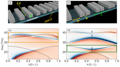
Here, we propose a novel one-dimensional topological graphene plasmonic crystal that consists of a monolayer graphene on top of a bulk substrate S with permittivity , separated from a periodic structure of silver rods with cross-section of area nm2 by a thin dielectric spacer, of thickness nm and permittivity (see Fig 1a). The main advantage of this structure is that it is based on a recent experimental setup to create graphene acoustic plasmons Iranzo et al. (2018), and therefore is experimentally feasible. The extra ingredient consists in using two different separations between the rods, which can be easily fabricated with the same techniques. Furthermore, it avoids the use of metagates Jung et al. (2018); Fan et al. (2019).
As illustrated in Fig 1b, the 1D lattice unit cell contains two identical silver rods separated by a distance and symmetrically located with respect to the center of the unit cell. Neighboring rods from different unit cells are separated by a distance . The periodic structure has a period . As dictates the intracell effective hopping and is linked to the intercell effective hopping, it is convenient to define the ratio that controls the topology of our system. ( Fig. 1a) implies the periodic structure studied previously Rappoport et al. (2020) with a single effective hopping. Positive (negative) values of specifies that the intracell effective hopping of our SSH model is larger (smaller) than the intercell one, as shown in Fig 1b.
We perform full-wave finite element frequency domain simulationscom (2018) and semi-analytical plane-wave expansions to characterize our plasmonic SSH model (see Supplemetary Materials for the details SM (2020)). For simplicity, graphene is simulated as a single layer with optical conductivity that is given by a Drude like expression Gonçalves and Peres (2016), where , is the Fermi energy, is the relaxation rate and is the frequency of the incident light. Since we will be considering large graphene Fermi energies, finite temperature play no significant effect in our results. The frequency-dependent relative permittivities of Ag are taken from Ref. Blaber et al. (2009).
First, we analyse the eigenfrequencies and eigenmodes of the system and distinguish their topological phases for different values of . We then proceed to describe the interaction of EM radiation with our MIG structure. We consider a -polarized monochromatic plane-wave impinging on the array of metallic rods at normal incidence. We calculate the absorption spectra resulting from the coupling of AGPs with far-field radiation, which can be used to design and model experiments. In this context, we consider different setups: a periodic system, an interface of two semi-infinite arrays with different topological phases, and edge states of a semi-infinite array interfacing a perfect electric conductor (PEC) . Unless otherwise specified, , eV and meV.
The dispersion of the plasmons in a periodic system with a single rod per unit cell of length presents several plasmonic bands Rappoport et al. (2020). If the same system is represented by a unit cell of length with two evenly located rods (), the dispersion can be depicted in a Brillouin zone which has half of the size of the original one. As a result of the band folding, the dispersions cross each other at , which is a point of degeneracy. When calculating the plasmonic band structure, from the analogy with a simple one-dimensional tight-binding SSH model, we should expect a splitting of the original bands for exactly at degenerate points of the band folding (that is, at ), with the size of the new gap being proportional to . This can be observed in our band structure and loss function calculations: figure 1c shows a density plot of the loss function calculated with the plane-waves expansion with a superimposed band-structure for . Each of the two original lowest bands for have one degenerate point at , which leads to a band folding induced band gap, splitting the original bands in two. The yellow rectangle in Fig. 1c highlights one of these band splittings, which is very small, because of the value of , but illustrates nevertheless the effect of the band folding. The new Bragg gaps for are always located at . Fig. 1d presents the same data but for and one can see that the band folding induced gap increases for large values of and there are four well separated bands labeled from 1 to 4. As expected, the band gap varies linearly with for small values of (see the supplementary material SM (2020)), and the band structures for are exactly the same, although they correspond to different topological phases.
The 1D array has chiral symmetry, as the unit cell consists of two interconnected sublattices (one for each rod) that can be interchanged without modifying the system properties. One-dimensional periodical systems with chiral symmetry can be characterized by a topological invariant known as Zak phase Zak (1989). If the unit cell has an inversion symmetry, the Zak phase is quantized as (non-trivial) or 0 (trivial). To evaluate the Berry phase for electromagnetic waves in the absence of magneto-electric coupling, either the electric or magnetic fields can be considered in the calculation of the Berry connection Onoda et al. (2006). We adopted the electric field in our calculations, where the permittivity tensor is isotropic and given by . After considering these simplifications, the Berry connection for an isolated band is given by Xiao et al. (2014); Wang et al. (2019):
| (1) |
where is the periodic-in-cell part of the normalized Bloch electric field eigenfunction of a state on the th band with wave-vector wavevector .
The periodic structure has periodicity in and the system is a one-dimensional plasmonic lattice. In this situation, the Zak phase Zak (1989) is defined as . The integral of the Berry connection over the BZ can be approximated as a summation of the contributions of small segments. If the BZ is divided into segments where , . As we are dealing with plasmons confined in the region between the metallic rods and the graphene sheet, without loss of generality, we can calculate the Zak phase at a fixed height located in the spacer with homogenous permittivity . The Zak phase of this segment for a band is given by
| (2) |
where can be calculated in a gauge-invariant formalism as Vanderbilt (2018).
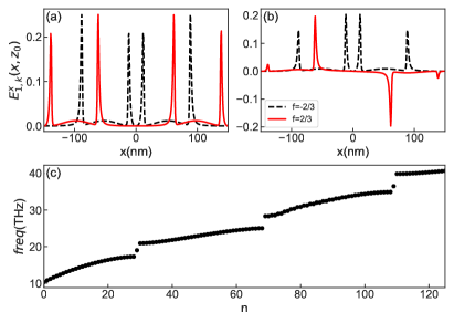
Alternatively, can be obtained by inspecting the parity of the field profiles. If the symmetries of the eigenmode at and are the same (different), the Zak phase of this band is quantized as (). Following this procedure, we illustrate the differences in the parity of the field profiles for band 2, highlighted in green in Fig 1d. Figure 2a, b presents the field profile and respectively. is located in the middle of the spacer, between graphene and the rods. The phase of the eigenmode is fixed in such a way that is real. For (Fig. 2a) the field profiles for are both even with respect to the inversion center of the unit cell, located at . On the other hand, for (Fig. 2b) the profile is even for and odd for . When comparing Fig. 2a and b it is clear that for () the symmetries of the eigenmodes for (a) and (b) are the same (opposite) so that , which corresponds to the value obtained by the Zak phase calculation following equation 2.
Lets us now address the physical consequences and experimental signatures of the Zak phase in the graphene plasmonic crystal. To obtain a clear signature of the topology, one route is the observation of interface states for different values of . Figure 2c shows the energy spectrum for a single finite system consisting of two neighbouring arrays of 20 unit cells each with respectively. The system is sandwiched by perfect electric conductors (PECs). As discussed previously, systems with the same have the same spectrum. Consequently, both arrays have the same band-structure and the spectrum of the four lowest bands for the composite system is similar to the unfolded version of the band structure of Fig 1d. However, there is a clear presence of mid-gap states inside the Bragg gaps. If two semi-infinite systems with different topological phases form an interface, the existence of a topological interface state in a given band gap is consistent with the bulk-edge correspondence. Thus, the mid-gap states of Figure 2c are associated to the different Zak phases of each individual array with , corroborating the previous analysis for periodic systems. The original bands for are split in two for but they do not cross any other band, independent of the value of . Because of the conservation of topological numbers in band theory, the sum of the Zak phases of each pair of these bands is always the same, regardless of the sign of , although each individual band can change its phase when inverting the sign of and the Bragg gap goes to zero. This results in the absence of mid-gap states in gaps located after an even number of bands (see Fig 2c).
To explore the experimental signatures of the Zak phase, we consider the coupling of the plasmonic crystal with far-field radiation. In this case, we have a -polarized monochromatic plane-wave impinging on the array of metallic rods at normal incidence. Let us first consider the periodic system and see if the splitting of the bands with different values of can be observed in far-field experiments. At normal incidence, TM modes couple with states with . Because of this, far-field experiments cannot directly obtain the linear dependence of the gap with , as the gap opening associated to the SSH model occurs at . Still, it is possible to capture: 1) the existence of an extra band for , and 2) the band separation at for increasing values of . The first bands that can be seen in the far-field experiments with normal incidence, are bands 3 and 4, highlighted in Fig 1 c. This is illustrated in figure 3a: the absorption spectra for has a single peak at this range of frequencies. For , the band is split in bands 3 and 4 and produces two peaks in the absorption spectra, where their position is dictated by the frequency of the bandstructure at . The peak separation is not directly related to the band gap but, instead, to the values of the band structure for .
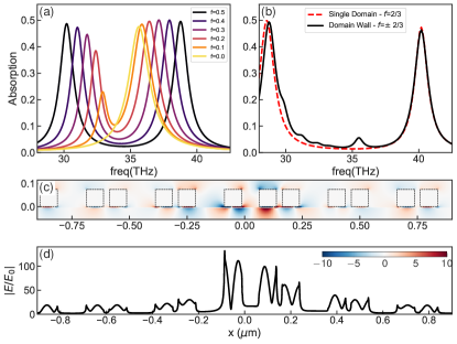
To analyse the interface states, we begin by considering a finite plasmonic lattice with with PEC ( perfect electric conductor) boundary conditions. This system presents exactly the same far-field response of the periodic lattice (see Fig. 3). We can now compare it with the response for the interface considered in Figure 2c, involving two joined arrays with . In this case, the interface state between different topological phases of the two chain leads to an extra absorption peak located between the two original peaks of the infinite system, seen in Fig. 3b. Figure 3c shows the field enhancement at the interface state at this particular frequency. The dashed squares indicate the position of the metallic rods and the interface between the two different lattices is located at . One can see that in the vicinity of the domain wall separating the two lattices, the field is enhanced in the whole space, including the region above the rods. Figure 3d exhibits the profile of , at , located in the spacer between graphene and the rods, where is the electrical field. In this case, the field enhancement is of the order of 120-140, which is of the order of the field enhancement of the main absorption peaks Rappoport et al. (2020). The electric field profile in Fig. 3c has a maxima that is strongly localized in the region of the interface between the two arrays. This differs from the extended electric field profile normally seen in the interface of photonic crystals with different Zak phases, where the interface state has a width of several unit cells Meng et al. (2018).
The topological nature of this peak can be further confirmed by comparing the absorption peaks of interfaces between two arrays with and where . In this case, one can produce interfaces between systems in the same topological phase (sgn()=sgn(). However, only interfaces between systems with sgn() sgn() produce interface states (see S. M). Although the topological nature of the bands cannot be easily tuned in-situ, it is still possible to use a gate to modify the optical conductivity in graphene. This leads to a change in the size of the band widths and gaps and the exact frequency of the edge state. The flexibility to modify the frequency of the interface state can be useful for technological applications.
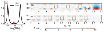
We can now consider a vacancy or a void in the unit-cell neighboring one of the PECs. This is obtained by removing the two silver rods belonging to the last unit cell of the right, as illustrated in Fig. 4b and c. In this case, the calculation of the eigenfrequencies of the finite system do not produce in-gap states that are related to the topology. Still, when analysing the interaction with far-field radiation, different responses emerge, depending on the Zak phase of the plasmonic band. For positive values of , there is an extra peak in the absorption spectra (Fig. 4a) which is related to an interface state and electric field enhancement of the electric field at the vacancy (Fig. 4b). However, for negative s, the absorption spectra is very similar to the periodic array and no interface states are observed. Instead, a resonator is formed between the last rod of the structure and the PEC. Depending on the size of the resonator, its eigenfrequency can be located inside the gap () or in the plasmonic band ), which explains the absorption spectra.
Although we cannot connect this response to topology, it can still be used in situations where one needs to produce a field confinement in the absence of the metallic rod, such as in sensing applications.
Conclusions We proposed a simple structure to simulate the Su-Schrieffer-Heeger Model for plasmons in graphene, which avoids the use of meta-gating . Our setup is based on Metal-Insulator-Graphene systems that host acoustic graphene plasmons. Periodic arrays of metallic rods with two rods per unit cell generate plasmonic bands with topological properties that can be tuned by the distances between the rods. Interface states with strong field enhancement can be created at the interface between two arrays with different topologies. The frequency of the localized state can be easily tuned by gating graphene, which opens new avenues in plasmonic applications where light needs to be confined to a precise location in space or where a tunable narrow band absorption is needed.
Acknowledgements.
TGR acknowledges funding from Fundação para a Ciência e a Tecnologia and Instituto de Telecomunicações - grant number UID/50008/2020 in the framework of the project Sym-Break and Mario G. Silveirinha for useful discussions. N.M.R.P. and F.H.L.K. acknowledge support from the European Commission through the project “Graphene-Driven Revolutions in ICT and Beyond” (Ref. No. 881603, CORE 3). N.M.R.P. acknowledge COMPETE 2020, PORTUGAL 2020, FEDER and the Portuguese Foundation for Science and Technology (FCT) through project POCI-01- 0145-FEDER-028114. F.H.L.K. acknowledges financial support from the Government of Catalonia trough the SGR grant, and from the Spanish Ministry of Economy and Competitiveness, through the “Severo Ochoa” Programme for Centres of Excellence in RD (SEV-2015- 0522), support by Fundacio Cellex Barcelona, Generalitat de Catalunya through the CERCA program, and the Mineco grants Ramón y Cajal (RYC-2012-12281, Plan Nacional (FIS2013-47161-P and FIS2014-59639- JIN) and the Agency for Management of University and Research Grants (AGAUR) 2017 SGR 1656. This work was supported by the ERC TOPONANOP under grant agreement n 726001 and the MINECO Plan Nacional Grant 2D-NANOTOP under reference no FIS2016-81044-P.References
- Hasan and Kane (2010) M. Z. Hasan and C. L. Kane, Rev. Mod. Phys. 82, 3045 (2010).
- Qi and Zhang (2011) X.-L. Qi and S.-C. Zhang, Rev. Mod. Phys. 83, 1057 (2011).
- Ren et al. (2016) Y. Ren, Z. Qiao, and Q. Niu, Reports on Progress in Physics 79, 066501 (2016).
- Wang and Zhang (2017) J. Wang and S. Zhang, Nature Mater. 16, 1062 (2017).
- Lu et al. (2014) L. Lu, J. D. Joannopoulos, and M. Soljačić, Nature Photonics 8, 821 (2014).
- Ozawa et al. (2019) T. Ozawa, H. M. Price, A. Amo, N. Goldman, M. Hafezi, L. Lu, M. C. Rechtsman, D. Schuster, J. Simon, O. Zilberberg, and I. Carusotto, Rev. Mod. Phys. 91, 015006 (2019).
- Silveirinha (2015) M. G. Silveirinha, Phys. Rev. B 92, 125153 (2015).
- Yang et al. (2015) Z. Yang, F. Gao, X. Shi, X. Lin, Z. Gao, Y. Chong, and B. Zhang, Phys. Rev. Lett. 114, 114301 (2015).
- Ma et al. (2019) G. Ma, M. Xiao, and C. T. Chan, Nature Reviews Physics 1, 281 (2019).
- Rider et al. (2019) M. S. Rider, S. J. Palmer, S. R. Pocock, X. Xiao, P. Arroyo Huidobro, and V. Giannini, Journal of Applied Physics 125 (2019), 10.1063/1.5086433, arXiv:1812.08679 .
- Ota et al. (2020) Y. Ota, K. Takata, T. Ozawa, A. Amo, Z. Jia, B. Kante, M. Notomi, Y. Arakawa, and S. Iwamoto, Nanophotonics 9, 547 (2020).
- Su et al. (1979) W. P. Su, J. R. Schrieffer, and A. J. Heeger, Phys. Rev. Lett. 42, 1698 (1979).
- Su et al. (1980) W. P. Su, J. R. Schrieffer, and A. J. Heeger, Phys. Rev. B 22, 2099 (1980).
- Rhim et al. (2017) J.-W. Rhim, J. Behrends, and J. H. Bardarson, Phys. Rev. B 95, 035421 (2017).
- Heeger et al. (1988) A. J. Heeger, S. Kivelson, J. R. Schrieffer, and W. P. Su, Rev. Mod. Phys. 60, 781 (1988).
- Xiao et al. (2014) M. Xiao, Z. Q. Zhang, and C. T. Chan, Phys. Rev. X 4, 021017 (2014).
- Gao et al. (2015) W. S. Gao, M. Xiao, C. T. Chan, and W. Y. Tam, Opt. Lett. 40, 5259 (2015).
- Wang et al. (2016) Q. Wang, M. Xiao, H. Liu, S. Zhu, and C. T. Chan, Phys. Rev. B 93, 041415 (2016).
- Henriques et al. (2020) J. C. G. Henriques, T. G. Rappoport, Y. V. Bludov, M. I. Vasilevskiy, and N. M. R. Peres, Phys. Rev. A 101, 043811 (2020).
- Ling et al. (2015) C. W. Ling, M. Xiao, C. T. Chan, S. F. Yu, and K. H. Fung, Optics Express 23, 2021 (2015).
- Downing and Weick (2017) C. A. Downing and G. Weick, Physical Review B 95 (2017), 10.1103/physrevb.95.125426.
- Gómez et al. (2017) D. E. Gómez, Y. Hwang, J. Lin, T. J. Davis, and A. Roberts, ACS Photonics 4, 1607 (2017).
- Li and Miroshnichenko (2018) C. Li and A. Miroshnichenko, Physics 1, 2 (2018).
- Pocock et al. (2018) S. R. Pocock, X. Xiao, P. A. Huidobro, and V. Giannini, ACS Photonics 5, 2271 (2018).
- Pocock et al. (2019) S. R. Pocock, P. A. Huidobro, and V. Giannini, Nanophotonics 8, 1337 (2019).
- Jung et al. (2018) M. Jung, Z. Fan, and G. Shvets, Phys. Rev. Lett. 121, 086807 (2018).
- Fan et al. (2019) Z. Fan, S. Dutta-Gupta, R. Gladstone, S. Trendafilov, M. Bosch, M. Jung, G. R. Iyer, A. J. Giles, M. Shcherbakov, B. Feigelson, J. D. Caldwell, M. Allen, J. Allen, and G. Shvets, Nanophotonics 8, 1417 (2019).
- Gonçalves and Peres (2016) P. A. Gonçalves and N. M. Peres, An Introduction to Graphene Plasmonics (2016) pp. 1–431, arXiv:1609.04450 .
- Jablan et al. (2009) M. Jablan, H. Buljan, and M. Soljačić, Phys. Rev. B 80, 245435 (2009).
- De Abajo (2014) F. J. G. De Abajo, ACS Photonics 1, 133 (2014), arXiv:1402.1969 .
- Park et al. (2015) H. R. Park, S. Namgung, X. Chen, N. C. Lindquist, V. Giannini, Y. Francescato, S. A. Maier, and S. H. Oh, Advanced Optical Materials 3, 667 (2015).
- Koppens et al. (2014) F. H. Koppens, T. Mueller, P. Avouris, A. C. Ferrari, M. S. Vitiello, and M. Polini, Nature Nanotechnology 9, 780 (2014).
- Low and Avouris (2014) T. Low and P. Avouris, ACS Nano 8, 1086 (2014), arXiv:1403.2799 .
- Celano and MacCaferri (2019) U. Celano and N. MacCaferri, Nano Letters 19, 7549 (2019).
- Alonso-González et al. (2017) P. Alonso-González, A. Y. Nikitin, Y. Gao, A. Woessner, M. B. Lundeberg, A. Principi, N. Forcellini, W. Yan, S. Vélez, A. J. Huber, K. Watanabe, T. Taniguchi, F. Casanova, L. E. Hueso, M. Polini, J. Hone, F. H. Koppens, and R. Hillenbrand, Nature Nanotechnology 12, 31 (2017), arXiv:1601.05753 .
- Lundeberg et al. (2017) M. B. Lundeberg, Y. Gao, R. Asgari, C. Tan, B. V. Duppen, M. Autore, P. Alonso-González, A. Woessner, K. Watanabe, T. Taniguchi, R. Hillenbrand, J. Hone, M. Polini, and F. H. Koppens, Science 357, 187 (2017), arXiv:1704.05518 .
- Iranzo et al. (2018) D. A. Iranzo, S. Nanot, E. J. Dias, I. Epstein, C. Peng, D. K. Efetov, M. B. Lundeberg, R. Parret, J. Osmond, J. Y. Hong, J. Kong, D. R. Englund, N. M. Peres, and F. H. Koppens, Science 360, 291 (2018), arXiv:1804.01061 .
- Gonçalves (2020) P. A. D. Gonçalves, Plasmonics and Light–Matter Interactions in Two-Dimensional Materials and in Metal Nanostructures (Springer International Publishing, 2020).
- Principi et al. (2011) A. Principi, R. Asgari, and M. Polini, Solid State Communications 151, 1627 (2011).
- Lee et al. (2019) I. H. Lee, D. Yoo, P. Avouris, T. Low, and S. H. Oh, Nature Nanotechnology 14, 313 (2019).
- Epstein et al. (2020) I. Epstein, D. Alcaraz, Z. Huang, V.-V. Pusapati, J.-P. Hugonin, A. Kumar, X. M. Deputy, T. Khodkov, T. G. Rappoport, J.-Y. Hong, N. M. R. Peres, J. Kong, D. R. Smith, and F. H. L. Koppens, Science 368, 1219 (2020).
- Rappoport et al. (2020) T. G. Rappoport, I. Epstein, F. H. L. Koppens, and N. M. R. Peres, ACS Photonics 7, 2302 (2020).
- com (2018) “Comsol multiphysics® v. 5.4,” (2018).
- SM (2020) “Supplementary material,” (2020).
- Blaber et al. (2009) M. G. Blaber, M. D. Arnold, and M. J. Ford, The Journal of Physical Chemistry C 113, 3041 (2009).
- Zak (1989) J. Zak, Phys. Rev. Lett. 62, 2747 (1989).
- Onoda et al. (2006) M. Onoda, S. Murakami, and N. Nagaosa, Phys. Rev. E 74, 066610 (2006).
- Wang et al. (2019) H.-X. Wang, G.-Y. Guo, and J.-H. Jiang, New J. Phys. 21, 093029 (2019).
- Vanderbilt (2018) D. Vanderbilt, Berry Phases in Electronic Structure Theory (Cambridge University Press, 2018).
- Meng et al. (2018) Y. Meng, X. Wu, R.-Y. Zhang, X. Li, P. Hu, L. Ge, Y. Huang, H. Xiang, D. Han, S. Wang, and W. Wen, New Journal of Physics 20, 073032 (2018).