Industrially Microfabricated Ion Trap with 1 eV Trap Depth
Abstract
Scaling trapped-ion quantum computing will require robust trapping of at least hundreds of ions over long periods, while increasing the complexity and functionality of the trap itself. Symmetric three-dimensional (3D) structures enable high trap depth, but microfabrication techniques are generally better suited to planar structures that produce less ideal conditions for trapping. We present an ion trap fabricated on stacked 8-inch wafers in a large-scale MEMS microfabrication process that provides reproducible traps at a large volume. Electrodes are patterned on the surfaces of two opposing wafers bonded to a spacer, forming a 3D structure with standard deviation in alignment across the stack. We implement a design achieving a trap depth of 1 eV for a 40Ca+ ion held at from either electrode plane. We characterize traps, achieving measurement agreement with simulations to within % for mode frequencies spanning 0.6–3.8 MHz, and evaluate stray electric field across multiple trapping sites. We measure motional heating rates over an extensive range of trap frequencies, and temperatures, observing 40 phonons/s at 1 MHz and 185 K. This fabrication method provides a highly scalable approach for producing a new generation of 3D ion traps.
- 3D
- three-dimensional
- PCB
- printed circuit board
- SOI
- silicon on insulator
- MEMS
- micro-electro-mechanical system
- CCD
- charge-coupled device
- CMOS
- complementary metal-oxide-semiconductor
- NA
- numerical aperture
- DC
- direct current
- AC
- alternating current
- RF
- radio-frequency
- UV
- ultraviolet
- DRIE
- deep reactive ion etching
- SEM
- scanning electron microscope
- SAM
- scanning acoustic microscopy
- imox
- inter-metal oxide
- OVC
- outer vacuum chamber
-
February 2022
Keywords: ion trap technology, industrial microfabrication, ion trap characterization, quantum computing, micro-electro-mechanical systems, scalable technology
1 Introduction
Quantum computing [1, 2] and measurement [3] constitute areas in which quantum systems can provide an advantage relative to classical devices. However, this advantage generally only becomes apparent once a sufficient system size is achieved, which presents a challenge to all technologies being used to pursue this advantage.
In the context of quantum computing, trapped ion systems represent a promising approach that fulfills the DiVincenzo requirements [4, 5]. Many of the most significant results in the field of trapped-ion quantum computing have been achieved using macroscopic linear traps, which hold tens of ions in a single potential well [6, 7, 8, 9]. In such systems, high fidelity qubit operations [10], long coherence times [11], and control over long ion strings with about 50 qubits [7, 12] have been demonstrated. However, in order to scale to systems with enough resources to suppress errors using error correction, a modular approach based on inter-connected sub-units will likely be required.
Two modular approaches are under consideration, and are promising for scaling to more than 100 ions. In the first approach [13, 14], separated ion trap modules are interfaced by establishing entanglement through photonic links, an approach that will eventually place strong demands on the reproducibility of traps that must operate reliably in many different setups. The second approach uses multiple trapping zones situated in a single trap structure [15, 16, 17, 18, 19], where zones are interfaced by shuttling ions between them using voltages applied to segmented electrodes [20, 21, 22]. Scaling up using these approaches has been challenging due to its complexity: the realization of precisely fabricated trap structures with large numbers of electrodes, and the task of wiring these up and controlling them.
The use of well-established microfabrication techniques [23], including those using micro-electro-mechanical system (MEMS) technology [24, 25], is very attractive to realize traps that meet the demands of complexity and reproducibility that are critical to both approaches. However, while deposition and structuring of patterned conducting and insulating layers on a surface is highly accurate and can achieve high levels of complexity (as for example in ref. [23, 26, 27, 28, 29, 15, 19]), these techniques are generally ill-suited to realize 3D structures extending beyond several in the out-of-plane direction. Therefore, many early investigations were constrained to a planar electrode geometry, which results in lower trap depth (typically 100 meV) and highly asymmetric field lines [29, 28], complicating the control of traps and making them more susceptible to ion loss [30, 31]. Demonstrations of multi-segment 3D trap electrode structures have been achieved by stacking multiple layers of laser machined or etched material [32, 33, 22, 34], however the methods used to produce these traps were not compatible with standard semiconductor fabrication. However, these have achieved trap depths above 1 eV which results in long ion storage times [7, 35], and have demonstrated higher levels of control in advanced tasks such as junction transport [33] and non-adiabatic ion transport [20, 21].
In this article, we describe the design, fabrication, and characterization of a microfabricated ion trap that, in contrast to monolithic microfabricated traps [36], combines surface-electrode structures on multiple, precisely aligned wafers that results in a 3D structure. This achieves a trap depth that surpasses the typical depth present in microfabricated surface-electrode ion traps by one order of magnitude. Fabrication uses a MEMS process on an industrial fabrication line, which realizes reproducible production that can be easily adapted to incorporate new designs. Our fabrication process is streamlined and suited for mass production, including assembly and packaging.
We characterize ion trapping performance by trapping 40Ca+ ions in a cryogenic apparatus that allows extensive variation of the trapping conditions. We compare measured trap parameters with the simulated model, establishing broad agreement over motional mode frequencies between 0.6 MHz and 3.8 MHz. Studies are also carried out over temperatures between 75 K and 300 K. We measure motional heating rates, finding them comparable to traps with ion-surface distance close to our value [37], and characterize stray static-electric and magnetic field components. We thus provide evidence that this MEMS technology is suitable for realizing ion traps for scaled-up quantum technologies.
2 Ion Trap Design and Fabrication
2.1 Trap concept and design
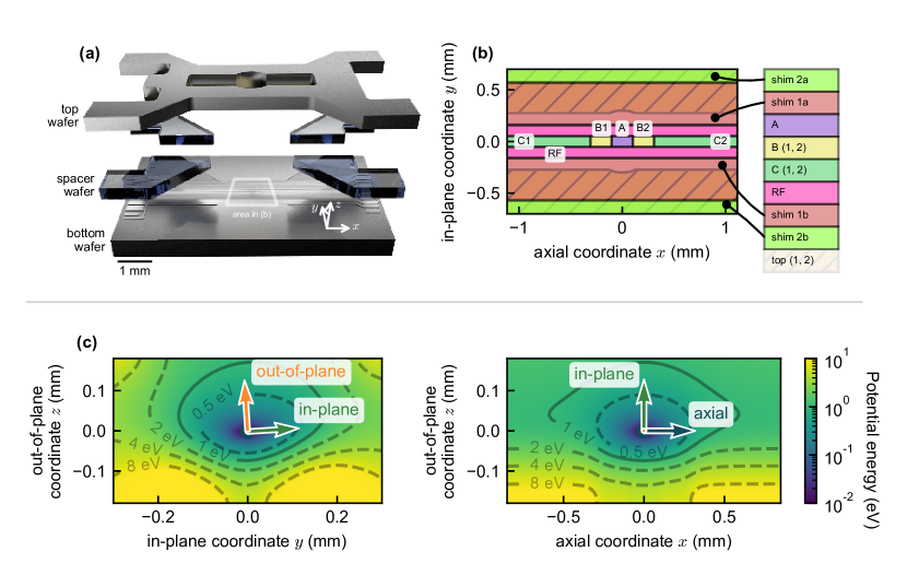
Our microfabricated 3D ion trap design, shown in Figure 1a, comprises three wafers. A bottom wafer carries direct current (DC) and radio-frequency (RF) signals on patterned segmented electrodes. Electrodes on the top wafer electrically extend the trap into the third dimension, creating a 3D structured trap. Our design serves as a proof of concept for a future 3D linear trap with RF electrodes on top and bottom wafers. Applying RF voltage to both bottom and top wafer allows for a more harmonic potential compared to surface-electrode traps and increases the intrinsic RF trap depth. As a first step towards this goal we incorporate DC electrodes on the top wafer to adjust the potential, including by redistributing confinement between the radial directions [38] to improve trap depth. A spacer wafer connects bottom and top wafer, and provides optical access. Such an electrode configuration is similar to previously realized surface traps with an additional metal lid on top to enhance trap depth [39, 40], but the presence of a patterned top wafer allows for extensibility and more complex control over the potential.
Electrostatic finite element method simulations were used to design the DC and RF electrode geometry shown in Figure 1b. The simulations consider the full potential in which a ion is trapped (over spatial coordinates indexed by r),
| (1) |
that includes the DC potential and RF potential in the pseudopotential approximation, wherein the force is time-averaged over an oscillation period of the RF drive [41]. The pseudopotential is given by
| (2) |
where is the elementary charge, is the atomic mass, and
| (3) |
for RF amplitude , RF frequency , and geometry-dependent factors adhering to Laplace’s equation for a linear Paul trap. In a simulation of the potential energy landscape, the trap depth is defined as the energy at the lowest saddle point in any direction away from the central trapping site at . If the ion’s energy exceeds this depth, it may escape the trap.
The trap typically operates at V and MHz. The overall trap depth was increased by biasing DC voltages so as to increase confinement into the out-of-plane direction () at the expense of confinement in the in-plane direction () [38], which does not generally limit trap depth in this design. The resulting voltage set solution, given in Table 1, produces the potential shown in Figure 1c, which remains highly harmonic around the trapping site (see A.1).
This potential gives a trap depth that is limited equally by 1.1 eV saddle points near to the and axes (at distances of and from the trap center, respectively), while the lowest potential barrier along the direction is 2.5 eV high around away. Higher trap depths could be reached if voltages were increased, ultimately limited by dielectric breakdown voltages between metal layers. In traps using a comparable layer stack-up and electrode spacing, breakdown voltages exceeding were measured [19].
The quadrupole confinement produced by this trap configuration can be compared to an ideal quadrupole potential (which has depth for dimensionless Mathieu parameter , using the conventions in ref. [42]) to extract a depth-parameterized trap efficiency in terms of intrinsic (RF-only) trap depth [38]. We simulate the potential of this trap with grounded top electrodes, as well as the planar-fabricated design in ref. [43], finding in both cases. This is comparable to 2–5% efficiencies calculated in other surface-electrode geometries [38, 44]. Similar results are to be expected, since the quadrupole field is generated similarly (in plane). Simulations of our microfabricated 3D trap predict an effective trap efficiency under operational conditions, when DC voltages are used to modify the radial potential. The intrinsic trap efficiency can be improved, for example, by applying RF drives to electrodes patterned on both top and bottom wafers. Our simulations show that electrode configurations can be found that produce a quadrupole potential similar to that of traditional 3D traps [45], with increased symmetry and trap depth relative to our present arrangement. However, while trap depth or trap efficiency are useful metrics for quantifying and comparing trap properties, additional benefits afforded by a 3D geometry — like increased symmetry and harmonicity — should be considered as well.
We also used simulation data to estimate mode frequencies, calculate stability parameters, predict the effect of static electric field offsets, and find electrode voltages that produce a specified electric potential. Convex optimization techniques were used to solve for voltage sets that could independently control axial confinement, rotation of the confining quadrupole of the potential in the radial plane, and micromotion compensation in three directions [46].
| 1 eV set (V) | 0.2 eV set (V) | |
| shim 2a | 0.04 | 8.16 |
| shim 1a | 11.32 | 0.24 |
| A | 7.66 | -1.07 |
| B (1, 2) | 8.95 | 5.29 |
| C (1, 2) | 17.18 | 4.91 |
| shim 1b | 12.77 | 1.28 |
| shim 2b | -24.03 | -9.04 |
| top (1, 2) | 10.46 | 0.58 |
| 183 | 155 |
2.2 Trap structure
The structure of the three stacked wafers comprising the 3D trap, including details on layer materials and thicknesses, is shown in Figure 2a.
The trap’s bottom wafer is based on a thick silicon substrate and uses the same multi-metal-layer technology used to produce a previous surface-electrode trap [19]. Axial confinement is provided by five segmented DC electrodes (‘A’, ‘B1’, ‘B2’, ‘C1’, ‘C2’) centered on the trap axis (Figure 1b) so that ions can be trapped along the axis at positions within of the center. DC compensation electrodes (‘1a’ and ‘1b’, which are displaced from the -axis and wide) on both sides of the trap axis run along the length of the trap and are used for micromotion compensation and radial rotation of the quadrupole moment of the potential. Two RF electrodes ( displaced from the -axis, wide) generate confinement in the radial direction. These are placed symmetrically along the axis and are connected together at one end of the trap. The remainder of the trap surface is taken up by DC electrodes (‘2a’, ‘2b’) that can be grounded or used for additional compensation. Vias between the three metal layers allow connections to electrodes at any location, such as the three isolated central islands, each long. The lowest metal layer shields the substrate to avoid RF loss in the silicon substrate [47] and aims to prevent the creation of charge carriers induced by stray laser light [48].
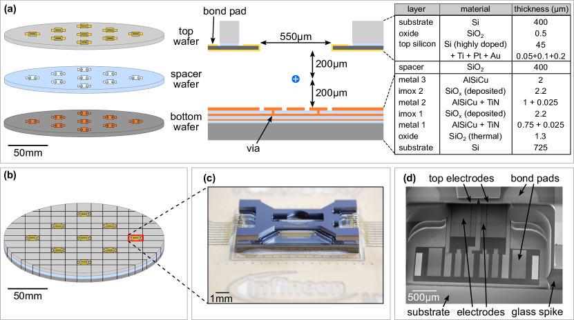
The top wafer consists of -thick highly-doped silicon on insulator (SOI). The highly doped silicon has a thickness of and a resistivity of at room temperature. This forms the top layer of the ion trap and incorporates two individually controlled DC electrodes. In this design, no RF is present on the top wafer. The top wafer electrodes are split to create a -wide slit, providing optical access to the ion with a numerical aperture NA that can be used for fluorescence detection. Two bonding pads on the top wafer allow for electrically connecting the top electrodes to additional bond pads on the bottom wafer or directly to the carrier printed circuit board.
The spacer wafer is made of -thick borosilicate glass featuring gaps at the sides and ends through which laser beams can pass above the surface, with an NA of 0.75 corresponding with openings away from the axis, and an NA of 0.2 along the axial direction. Additionally, wirebond pads at the ends of the trap are spaced to allow axial beam access. Thus, beams should be able to cross the center of the trap in the plane without obstruction at angles up to from the -axis, and about from the trap () axis.
2.3 Trap fabrication
In order to realize the 3D trap structure described above, three individual 8-inch wafers were wafer-bonded, as illustrated in Figure 2b. Fabrication of the ion trap was carried out in an industrial cleanroom facility 111Infineon Technologies Austria AG, Villach, Austria.
The silicon bottom wafer comprises three AlSiCu metal layers created via sputter deposition. These metal layers are isolated by inter-metal oxide (imox) layers, deposited as silicon oxide. All metal and oxide layers are structured by optical lithography followed by plasma etching. Details on the fabrication process for this technology can be found in ref. [19].
The -thick top electrodes and the -thick undoped silicon substrate of the top wafer are etched via deep reactive ion etching (DRIE), with an additional recess of the substrate silicon to provide the high NA (see the cross section in Figure 2a). To shield the ion from silicon surfaces, the electrodes are gold coated on both sides using a shadow-mask-evaporated stack of titanium, platinum, and gold. Here, titanium serves as an adhesion layer and platinum as a diffusion barrier between the gold and the silicon substrate. However, there are areas of exposed substrate silicon () on the top wafer, which, if charged up, could lead to stray electric fields at the ion’s position.
The spacer wafer is made of borosilicate glass with a coefficient of thermal expansion matched to silicon to minimize strain at cryogenic temperatures. All glass structures are created by a wet-chemical etch of from front and back sides, giving rise to an wide spike on the sidewalls (visible in Figure 2d). One concern this raises for the operation of the trap is that the uncoated glass surfaces could possibly lead to undesired stray charge buildup, causing additional electric fields, or lead to increased motional heating [49]. We study this effect in Section 3.2.
2.4 Wafer bond, dicing and assembly
Anodic wafer bonding [50] is a widely used method in industrial packaging and manufacturing, especially in the field of sensor systems [51, 52]. With its high bonding strength and robustness [53], it provides a suitable technique to connect individual wafers to form a 3D ion trap.
We developed a two-step anodic bonding process, optimized for inclusion in the industrial fabrication line: first, the bottom wafer is bonded to the glass spacer, and subsequently, the resulting double stack is bonded to the top wafer. This two-step process allows for semi-automatic optical alignment of both interfaces despite the opacity of silicon wafers that form the outer layers of the triple stack. We found optimal bond parameters of bond temperature and a bond voltage of , as verified by scanning acoustic microscopy (SAM) analysis, die-shear tests, and repeated cryo-cycling between room temperature and (within ca. 5 hours) or (within ca. 1 minute).
The ion traps on the bonded wafer are separated by mechanical dicing as shown in Figure 2b. Then, each ion trap is glued and electrically connected to a carrier PCB as part of an industrial packaging process, based on automated lead-frame handling, semi-automatic die-attach and automated wirebonding, resulting in the final chip shown in Figure 2c.
Using SEM imaging of the wafer stack cross section (Figure 2d) the bond alignment accuracy of 3–4 for each interface was verified. The standard deviation in the alignment tolerance of across the full wafer stack is in agreement with the lithographic and bonding tools’ specifications. A tilt between top and bottom wafer caused by variations in the glass wafer thickness () can be neglected for a single chip.
In the batch of traps characterized in this work, SEM imaging revealed a fabrication defect where the two top electrodes were connected together. Only the four shim (‘1a’, ‘1b’, ‘2a’, ‘2b’) and two top (‘top 1’, ‘top 2’) electrodes have significant radial potential moments that can rotate the quadrupole of the potential. Without this moment from individual top electrodes, higher voltages had to be applied to the shim electrodes to rotate radial modes, which limited the rotation angle of the modes seen in Figure 1c. Repeated analysis verified that the defect was corrected in later batches.
Trap fabrication can be done at high volume. Following introduction of the design into the production line, a one-time run-through of the manufacturing cycle (including packaging) produces 50 identical ion traps from one wafer in 4–6 weeks. Typical fabrication runs include lots of 25 wafers.
3 Experimental characterization
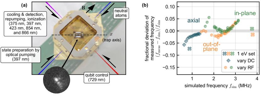
Measurements of traps with ions can validate the simulation, design, and fabrication process. We test our traps by placing them at the lowest-temperature (“base”) cooling stage of a cryogenic apparatus [54] and trapping ions. Traps are attached to a DC filter board (with first-order, 36 kHz-cutoff-frequency low-pass filters). DC signals are generated, pass through additional filters at room temperature, and are delivered to the base stage via flexible PCB ribbons to the trap filter board. These ribbons also carry lines from the DC voltage source that reference both DC and RF ground on the trap. The RF signal is delivered via coaxial cables and stepped up using a helical coil resonator (anchored to the same temperature stage, close to the trap), which sets the preferred RF drive frequency. The magnitude was inferred using a rectifier on the filter board PCB (B.1). A magnetic field G provided by external coils splits the energy levels of trapped ions using the Zeeman effect and defines a quantization axis. Lasers for photoionization, detection, cooling, state preparation, and qubit manipulation enter the trap structure along the directions as shown in Figure 3a.
This work describes two traps (#1 and #2) from the same fabrication batch tested sequentially in the cryostat, which was operated at a base cooling stage temperature K. The first trap was attached to a PCB that was directly thermally anchored to the base cooling stage. The second trap was placed on a PCB that included a calibrated Pt1000 thermistor, and was more weakly thermally linked to the cooling stage in order to allow characterization of the trap at temperatures up to . This thermistor permitted measurements of the trap temperature , calibrated as described in B.2, as well as application of a current to heat the trap independently of the entire base cooling stage.
Application of an RF drive frequency MHz at introduced a heat load W in both traps, likely originating from dissipation on the trap. In trap #2, where was measurable, this raised to . The RF dissipation may come from DC resistance of the RF electrodes (about at ) as well as dielectric loss from the large trap capacitance (about ), which could be mitigated through adjustments to materials and design geometry. We observed that our RF drive applied across this capacitance also produced large oscillating magnetic fields resulting in AC Zeeman shifts [55] of the levels in the transitions that we used for qubit manipulation. These shifts varied as the RF drive power was adjusted, giving rise to a 3.5% correction factor for a transition with (denoting spin quantum number ) for our values of RF drive and magnetic field. Our calculated magnitude of AC magnetic field at V, G, is about five times larger than has been reported in another microfabricated trap where this effect was also observed [56]. Most measurements required that we properly account for this effect.
Though we did not perform a systematic study, we observed that single ion storage times were shorter at higher trap temperatures, ranging from days (at trap temperatures close to K) to hours (near K). However, we did note that at a trap temperature K, strings of more than 10 ions could be trapped stably for days without ion loss. These three temperatures, from lowest to highest, corresponded with steady-state outer vacuum chamber (OVC) of , , and mbar as measured on a pressure gauge. This suggests that particles may have been generated near the area of increased temperature — perhaps desorbed from trap or heater surfaces — increasing the pressure locally, then eventually registering on the chamber pressure gauge. Ion loss may relate to collisions stemming from more plentiful or energetic particles [7]. These general observations occurred when either 0.2 eV- or 1.0 eV-depth voltage sets were applied, and so some effect besides trap depth, such as laser cooling capability, was more likely the primary factor contributing to ion loss.
3.1 Probing motional mode frequencies
To identify secular motional frequencies of a single trapped ion, we apply a voltage configuration, compensate micromotion, and then perform spectroscopy on the motional sidebands of a chosen transition. Here we present the data for trap #2, for which the most extensive characterization was performed. From the 1 eV voltage set in Table 1, we simulate mode frequencies MHz, ordered by the mode vectors closest to . Applying this voltage set, measurement of the trap gives frequencies MHz, consistent with the expected potential to within 8% axially and 2% radially (Figure 3b, ‘X’ markers). We next applied the 0.2 eV voltage set in Table 1, whose lower voltages provide more leeway for parameter variation without reaching voltage limits, and varied RF amplitude (changing radial frequencies) and DC voltages that modify axial curvature (changing axial frequencies). Over a set of parameters producing frequencies in the range 0.6–3.8 MHz, measured frequencies matched with simulated values to within 10% for the axial mode and 5% for radial modes (Figure 3b).
Uncertainty in applied likely dominates the radial frequency mismatch in Figure 3b. Stray electric field curvature, which is not included in these simulations, would explain a deviation in axial frequencies. Using sideband spectroscopy, we measured a residual anti-confinement (corresponding with axial frequency ) at the center trapping site in trap #2. Possible sources of such fields are discussed in Section 3.2. In any case, these observations validate the designed model over a wide range of parameters, consistent with high-depth traps that meet the design goals of our 3D microfabrication process.
3.2 Measuring stray static electric fields
Dielectric surfaces that are not electrically shielded from the ion can generate stray electric fields [49]. Stray fields that are not sufficiently stable or homogeneous may not be compensated well enough to perform high-fidelity quantum gate operations [57], and could make it difficult to scale this technology. To measure stray fields, we primarily use parametric-excitation-based micromotion compensation techniques [58]. From trap simulations, we infer the stray field corresponding to the applied micromotion compensation voltages. Our implementation is sensitive to V/m radial and V/m axial static electric fields. We characterize the fields present in both traps along the axis at different trapping sites (Figure 4a).
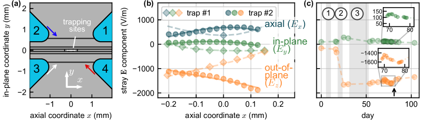
The results (Figure 4b) show large offset field components (up to about V/m in the out-of-plane direction) with about V/m axial variation along the measured distance range of mm from the trap center. The magnitude of field components in both traps is similar to many single-wafer surface traps [46, 59, 60, 30, 61, 62, 43, 19] made from a variety of materials and measured at different temperatures and ion-surface distances. Proposed sources of such fields include charge present on dielectric or metal surfaces [63, 64, 65], as well as patch potentials comprising surface oxides [66, 49] or adsorbates [67, 68, 69]. These sources can contribute to field offsets if they are distant or distributed, or to field curvature if they are close and point-like.
Since the stray field is inferred from the micromotion compensation required to move the ion to the RF null, trap misalignment that offsets the RF null can be mistaken for an offset field. This primarily affects lateral () offsets, which from the measured misalignment gives a standard deviation V/m. Uncertainty in the position of the null above the surface is dominated by spacer wafer thickness, , to give V/m. The measured misalignment contributes negligibly to axial field uncertainty. While misalignment could account for part of the offset of the measured fields, it cannot explain deviations larger than or over the range of trapping positions.
In contrast to surface-electrode traps, one possibly significant source of electric field could be charges on the sidewalls of the spacer wafer. The data in Figure 4b (lines) are fitted to the simulated field from uniform charge densities on these sidewalls, producing values up to 2500 elementary charges per (Table 2). This is larger than the charge densities reported on fiber surface near ions [65] and on a planar trap [63], but these materials and geometries may not be comparable. The model uses seven free parameters: a uniform charge density on each of the spacers 1–4 that control field curvature along the axis, and the three components of a constant, arbitrary field that set the offset. Additional variability of 400 in charge density and 200 V/m in may come from simulated field uncertainty, considering that the spiked sidewall’s position (Figure 2d) has a standard deviation due to an uncertain etch profile.
The field offsets could be explained, for example, by a charge density of in the gaps between electrodes on the bottom wafer, which we find in simulation to produce an out-of-plane field offset close to the V/m measured at the center trapping site. Though this exceeds the charge density that would be required on the spacer sidewalls to produce a comparable field, this field magnitude is nonetheless common among microfabricated surface-electrode traps without significant exposed bulk dielectric [46, 43, 19], and so such surface-based field sources cannot be ruled out. Due to the relative asymmetry of the trap in the out-of-plane direction, these effects all tend to produce larger field components along , which is consistent with the measured data. If this charge were unevenly distributed, or debris were present on a trap surface, this could provide curvature in addition to an offset field.
Offset fields might also come from far-away structures that are not part of the trap assembly, like charged lenses or windows. Calculations predict that fields from the nearest dielectric surface (43 mm away) would be shielded by a factor of by the largest aperture ( mm) between the dielectric surface and the ion. The trap is otherwise surrounded by grounded conductors. Therefore, sources of electric field within the shielded region are most consistent with the observations.
| trap #1 | trap #2 | |
| charge densities | ||
| spacer 1 | -2120(340) | 1380(200) |
| spacer 2 | 860(400) | 630(360) |
| spacer 3 | 1840(380) | -2510(450) |
| spacer 4 | 390(260) | 320(250) |
| offset fields (V/m) | ||
| -450(50) | 1310(40) | |
| -380(50) | 210(50) | |
| -900(170) | -1500(40) |
The sources responsible for these electric fields may be intrinsic, induced by light, or introduced by atomic flux while operating the trap. Some light from the laser beams that pass through the trap (Figure 4a, blue and red arrows) was observed to scatter from the trap’s inner surfaces and the sides of spacers 2 and 4. If this induced charge, we would expect the strongest effect from the deepest- ultraviolet (UV) wavelength, photoionization light, present at during loading. During loading, neutral calcium also travels along the direction indicated by the white arrow in Figure 4a, and can deposit on trap surfaces including the sides of spacers 1 and 3. Adsorbate build-up has been shown to alter stray fields [70, 56]. However, we observe that the field remains stable during trap operation, and we do not observe significant stray field drift in the seconds or hours after loading (resolvable by tracking the ion’s position on a camera). Therefore, while induced charge on these surfaces may contribute to part of the measured field, the bulk of the charge appears to be intrinsic.
We observed small day-to-day changes, culminating in weekly field drifts of 10 V/m in-plane and 100 V/m out-of-plane (Figure 4c), which could be explained by local charging and dissipation or fluctuations of DC voltages. These fluctuations were small relative to the axial position field dependence in Figure 4b. Special events like long-term electrical outages, or vacuum or thermal cycling, produced changes at a faster rate. In one such case, a significant change in measured field occurred after DC electronics were disconnected and reconnected. This could have possibly reconnected floating electrodes (thus changing the calibration of applied compensation or affecting the charge state of weakly implanted electrons in dielectric close to the electrodes [65]) or changed the contact potential at a conductor interface. We note that after the jump the compensated field drift was observed to reverse direction. None of these events are likely to have removed adsorbed surface contaminants.
Overall, the behavior of stray electric fields is similar to that seen in other microfabricated traps, which is consistent with models of charge on bulk dielectric (in our case, for example, spacer sidewalls), in dielectric gaps, or on conductor surfaces in the electrode plane. The observed fields exhibit low drift and are well within the range that can be compensated using low voltages ( V) applied to the available DC electrodes, and thus they do not present an obstacle to trap operation that could hinder the scaling prospects of our 3D MEMS ion trap technology.
3.3 Heating rates
Motional heating of ions reduces the fidelity of single-qubit gates and multi-qubit entangling operations [57] that are critical to a trapped ion quantum processor [71]. Heating of the ions’ motional modes occurs at a rate due to electric field noise [72]. This rate can be related to the electric-field noise spectral density, , using [73]
| (4) |
where is the ion mass, the mode frequency, and the electron charge. We measure heating rates of a single ion’s axial, in-plane radial, and out-of-plane radial motional modes using the sideband ratio method [74]. By comparing the (or ) dependence on mode frequency, trap temperature, and system configuration to known models, we can pinpoint noise sources and evaluate trap performance. In addition, we monitor drift and scatter of heating rates over time, as well as the response to micromotion miscalibration.
Measured heating rate data are shown in Figure 5, plotted against mode frequency , trap temperature , and radial mode angle . To access all modes with laser beams propagating parallel to the plane of the trap, we employ voltage sets (starting with the 0.2 eV-deep set in Table 1) that rotate the radial modes by an angle relative to and using the off-axis shim electrodes. The lowest measured heating rates are below 10 phonons/s at 2.6 MHz at K and around 40 phonons/s at 1.0 MHz at K; using Eq. 4 these evaluate to electric field spectral noise densities of and , respectively. These heating rates are close to those measured elsewhere [73, 37] when comparing to traps with similar ion-electrode distance (). These measurements were taken in trap #2. While trap #1 produced heating rates as low as 26(2) phonons/s for a radial mode at 2.6 MHz, the trap temperature could not be estimated on this device, and calibrations were not performed as systematically as for trap #2. Therefore, all heating rate data presented here was measured using trap #2.
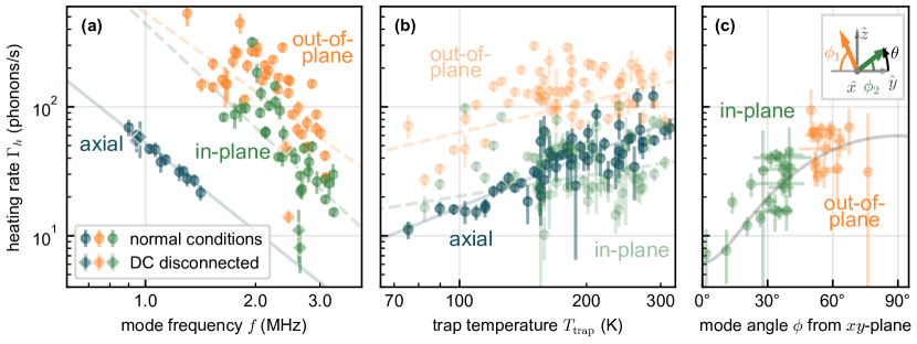
In Figure 5a–b, axial mode data exhibit low scatter, while radial mode data are more scattered relative to the low uncertainty at each point. The uncertainty of individual measurements is obtained by applying binomial statistics to a series of ‘bright’ or ‘dark’ determinations from thresholding photon detection events within a detection window [75]. The plotted uncertainties represent the standard errors of the mean of fitted heating rates for multiple such measurements. The axial mode heating rate follows a power-law scaling model with respect to both temperature and frequency, for exponents of mode frequency (, Figure 5a) and temperature (, Figure 5b). Fits of the axial heating rate data to and give and respectively. Literature values are often given in terms of scaling coefficients and , which are related through to give and . Our scaling exponents are similar to those given in other work [76, 77, 66, 49], in particular the , seen to result from electric field noise from surfaces, for example as in ref. [78]. We cannot access low enough trap temperatures to distinguish whether the temperature scaling remains unchanged below our lowest measured temperature, 75 K, or the temperature scaling is disjointed as in ref. [79, 80].
The scatter in radial heating rates in Figure 5a is consistent with the effect of a “technical” noise source, with many distinct spectral features that collectively contribute to a large background rate. In the presence of such a source, one would expect an ion to exhibit higher heating rates when its motional frequency is tuned closer to frequency peaks in the electric field noise spectrum. When fit to a power law model, we find exponents and for in-plane and out-of-plane modes; the expected frequency dependence would depend on the nature of the external noise source. This scatter behavior is also consistent with data in Figure 5b, where radial heating rates are not significantly correlated with trap temperature that was adjusted using a heater. In this case, one would expect trap temperature to affect modes for which surface-based noise sources limit the heating rate, while trap temperature would hardly change the effect of external sources. This points to an externally generated noise source, which may be carried along transmission lines to the DC electrodes [73].
Normalization of heating rates was performed in some cases to easily compare data sets collected where different DC or RF voltages were applied, or where trap impedance was modified by the temperature, thus slightly changing delivered power, altering RF amplitude, and shifting motional mode frequencies (see C.1). Heating rates measured while sweeping the trap temperature in Figure 5b were frequency-normalized to the mean frequency values of axial, out-of-plane radial, and in-plane radial modes, MHz. Heating rates in Figure 5a were not temperature-normalized, however, since axial mode rates were taken at a constant temperature and radial mode rates were not strongly correlated with temperature (C.1).
We noted that the scatter of radial mode heating rates in Figure 5a–b was consistent with a technical noise spectrum that may originate externally; however, temporal variation of noise sources could also produce scatter. To check this, we repeatedly interleaved calibrations and heating rate measurements over nearly 8 hours (with 8 measurements at 43 minute intervals followed by 10 measurements at 13 minute intervals) at K and at mode frequencies MHz. Over 19 sequential measurements, this gave mean values of , , and phonons/s for axial, out-of-plane radial, and in-plane radial modes, and standard deviations , , and phonons/s, respectively (see C.2). Despite significant axial rate uncertainty under these conditions, the standard deviation of radial rates is small. This suggests that radial heating rate scatter is not the indirect product of drifts in noise properties over time. Seven measurements were performed in the presence of radial shimming fields up to V/m, which displaced the ion about from the RF null. They did not show a strong dependence on the stray field magnitude, and gave respective mean values , , and phonons/s, and standard deviations , , and phonons/s, respectively. This suggests that neither noise delivered through the RF electrodes nor drifts in static stray fields over time play a significant role in the measured heating rates.
The data in Figure 5a–b are taken at an angle of the radial mode vectors about the trap axis. To understand the effect of this angle, we applied DC voltage sets that adjusted from to . This sets each mode’s angle with respect to the -plane (Figure 5c inset). The ion excitation signal while driving motional sideband transitions also depends on this angle through an effective Rabi rate sensitive to the angle between the beam wavevector and the mode [41]. From these measurements, we cross-checked the designed angle and obtained uncertainty values. As a mode approaches (out of the plane and orthogonal to the cooling beams) sideband cooling performance degrades, higher initial photon numbers are measured, and the uncertainty of heating rates using the sideband ratio method increases. Therefore, for each mode, data collection is conditioned on cooling to initial values of average photon number , and also on confidence in mode frequency from a calibration using sideband spectroscopy (requiring standard error ). Even with these conditions, a few outliers result (for example, with negative rates or >400% relative uncertainty), which are omitted from the plots for clarity. To directly examine the dependence of heating rate on , frequencies are normalized to the mean frequency of both radial modes’ data (3.00 MHz) using the procedure described above. The resulting data (Figure 5c) show that heating rates increase significantly as rotates from an in-plane orientation (along ) to an out-of-plane orientation (along ).
These measured heating rates can be described by a sinusoidal model that gives rates at ten times lower than at . If electric field noise at the ion were limited by losses in a surface dielectric or metal film, one would expect out-of-plane rates two times larger than in-plane rates [78]. The observed excess scaling, however, is more consistent with a model of noise delivered from an external source, such as through trap electrodes. By symmetry of this trap’s electrode layout and its asymmetry in the out-of-plane direction, voltage noise common to all DC electrodes would produce electric field components that are normal to the electrode planes.
Considering whether externally generated noise may couple to the electrodes through DC wiring and limit the heating rates measured on radial modes, we adjusted the DC electrical configuration (further details given in B.3). We found that radial heating rates were only significantly reduced when disconnecting the trap from its DC voltage sources and ground references (which also reference the RF ground). Disconnection left the electrodes electrically floating, with the capacitance of the electrodes and DC filter board capacitors maintaining a nearly constant voltage over time.
With DC lines disconnected (Figure 5a, diamond points) the radial heating rates drop, nearly reaching the frequency scaling trend line set by the axial mode. Even when normalizing for frequency, the average in-plane rate remains below the out-of-plane rate by a factor of 2.3, which is almost consistent with noise due to a bulk dielectric or surface layer noise models [78, 49]. However, the two out-of-plane data points (which are taken at slightly different frequencies and temperatures) still demonstrate scatter exceeding the measurement uncertainties. This scatter and the discrepancy in the ratio of the radial modes’ rates suggest that some technical noise sources may persist and become dominant when the DC voltage sources are externally disconnected. These may include inductive pick-up within the cryostat or noise on the RF electrodes.
Heating rates of the axial mode were unaffected by the disconnection of an external noise source, which along with its frequency and temperature dependence suggests a limiting noise source originating on trap surfaces or in bulk dielectric. The relatively low spectral noise densities of this source suggest that our MEMS ion trap technology does not face an exceptional obstacle to scaling due to surface material composition or other aspects of the fabrication method. Radial heating rates, on the other hand, appear to be dominantly set by noise sources originating externally to the trap as evidenced by their scatter, trap temperature independence, strong out-of-plane polarization, and response to DC disconnection. Regardless, for the purpose of trap characterization, these measurements place an upper bound on the contributions from trap surface-based noise sources. Improvements to the apparatus would reduce technical noise and improve the radial modes’ sensitivity to remaining sources of noise, benefiting further trap characterization.
4 Conclusion and Outlook
We have demonstrated the operation of a microfabricated MEMS 3D ion trap with a trap depth of 1 eV produced in an industrial facility. Measurements of motional frequencies agreed to within % of predicted values over a broad range of DC and RF voltages, validating our simulation model and suggesting that the trap was accurately fabricated. We found motional heating rates (<40 phonons/s at 1 MHz axial frequency) commensurate with electric field noise spectral densities found in surface traps of this scale [73, 37]. Our traps could be operated stably, with strings of more than 10 ions trapped for days at lower trap temperatures. Though the data presented was only measured at trap temperatures as low as 70 K due to RF dissipation on the trap, stronger thermal anchoring to the base cooling stage operating with 1.5 W of cooling power at K or changes to trap materials and geometry should further reduce heat load. We also characterized the trap up to temperatures of 300 K, suggesting that room temperature operation is possible with this technology.
Because the traps were measured in a newly constructed cryogenic trapping apparatus for which noise had not previously been characterized [54], we discovered systematic noise consistent with an external source. We further isolated this noise, identifying that the electrical configuration (primarily, grounding related to DC voltage supplies) played a role, which indicates the need to improve source noise levels, external filtering, and grounding configuration. Considering the remaining sources of noise, we found an axial mode heating rate dependence on mode frequency and trap temperature in accordance with models of surface effects like fluctuating patch potentials or electric field noise from dielectric bulk or surface layers. We also observed the presence of a large stray static electric field, finding that it was stable and could be compensated. Stray electric fields of this magnitude are sometimes linked to high heating rates [60], but we do not observe this.
Our observations may also inform the design of the next generation of 3D-structured microfabricated ion traps. For example, we observed that isotropically etched spacers produced sharp sidewall profiles, creating light scatter and possibly contributing to stray electric field that needed to be compensated. These walls could be surface-treated, retracted, or flattened using different etching techniques (while ensuring mechanical stability) in order to reduce any limitation on heating rates due to surface dielectric effects. If noise sources originate in bulk dielectric such as these spacers, metal shielding layers could mitigate them. Material and design engineering approaches, for example by thickening metal and dielectric layers, could lower ohmic and capacitive loss through the RF electrodes, reducing power dissipation and lowering the temperature at which the trap can be operated.
The MEMS microfabrication process used to construct the trap in this work is extensible, supporting a number of technologies that will manage growing complexity. Connectivity between the trap and signal or measurement lines could be handled using through-substrate vias [81], while through-glass vias [82] could replace wirebond connections between wafers. By integrating on-chip electronics [83], one could increase signal density without increasing in-vacuum wiring requirements or burdening cryostats with excess heat loads. Integrated waveguides [43, 84] would allow to channel light used for trapping, cooling, detection, and control to the ion, thus relaxing requirements for optical access. Junctions could be patterned along the trap axis [32, 33, 21, 62, 34] to interface zones, though the spacer and top wafers must be designed carefully to allow optical access. Through the use of vias and multiple metal layers, both top and bottom wafers support extensive electrode segmentation, which could extend to include the addition of RF rails on either wafer. Multiple trapping zones and RF rails have been demonstrated using this technology in surface traps, including in a single-wafer predecessor of this trap [19]. Work to integrate several of these technologies into our microfabricated MEMS trap is actively underway.
Our demonstration of an industrially microfabricated trap with high performance, stable operation, and the potential to integrate optical and electronic features thus positions 3D MEMS ion traps as a promising technology with which to underpin a scalable approach to trapped-ion quantum computing.
Appendix A Simulation methods
A.1 Potential symmetry and anharmonicity
In Section 2.1 we investigated the effect of applying DC voltages to increase confinement into the out-of-plane direction () at the expense of confinement in the in-plane direction (). The resulting voltage set solution, given in Table 1, produced the potential shown in Figure 1c, which remains highly harmonic around the trapping site. In particular, the ratio of the fourth-order term to the second-order term of an even polynomial fourth-order fit to the pseudopotential are 0.6%, 0.7%, and 8% at trap coordinates , , and relative to the trap center, respectively. These distances are chosen because they (in the axial direction) represent the extent of a reasonable ion chain, and (in the radial directions) are on the order of the ion-electrode distance. The effect of fourth-order anharmonicity sampled closer to the trap center will be smaller, since it scales with . These results are not significantly changed from the case with less out-of-plane confinement (the 0.2 eV voltage set in Table 1), with ratios 0.6%, 0.8%, and 12%. From the change in out-of-plane asymmetry between the two voltage sets, it appears that the use of DC to modify confinement improves the symmetry, which is to be expected since this produces a more quadrupole-like pseudopotential with larger effective trap efficiency. From exploratory simulations, we see that of RF drives on electrodes on the top wafer have a similar effect, but by modifying the intrinsic trap efficiency.
Appendix B Experimental methods
B.1 RF voltage calibration
Values of were inferred primarily using a rectifier circuit that sampled a fraction of the RF signal near the trap. Using values of the circuit components specified to 1% uncertainty, the rectifier signal was used to calibrate the temperature-dependent transfer function of the resonator used to step up the RF voltage. However, the pick-off fraction of the rectifier is also temperature dependent, increasing this uncertainty to about 5%.
B.2 Trap temperature calibration
We found to be a good proxy for the temperature of the bottom wafer trap surface (on which the RF electrodes were present) when the thermistor was also used as a heater over the range 75–300 K. We used a temperature-dependent signature of the complex-valued RF reflection signal to calibrate , and then relate this to . The RF signal is delivered to the electrodes via a coaxial transmission line, through a step-up resonator, and then through intermediate PCBs onto the trap chip. We want to access the portion of the signature that depends only a change in temperature of the trap chip.
First, we slowly cooled the cryostat from 300 K to 7 K, with no current flowing through the Pt1000 thermistor and no constant drive applied to the RF electrodes, and measured the temperature near the RF resonator , the temperature on the intermediate PCBs , and . Under these conditions, the temperatures of these thermometers — all at the cryostat base temperature stage — were assumed to be in equilibrium, including with and . (This also served to calibrate .) Further, our RF resonator is constructed using internal coils soldered to a outer body, and so we expect the whole structure to be well thermally connected at a temperature well represented by . Therefore we know the temperatures of the different elements in the RF circuit that could each contribute to .
Once the cooldown calibration was complete, and cryostat had settled at a base temperature, we used the trap thermistor to raise over a range 7–300 K. Correspondingly, and only increased from to below , suggesting that changes in the RF impedance of the trap, rather than the resonator or other parts of the circuit, were primarily responsible for the behavior of . The center frequency and width of the resonance were extracted from over the range of the cooldown calibration, which vary monotonically with , to be used as a signature with which to infer . Finally, while heating the thermistor, the inferred surface temperature was seen to agree with to within , suggesting that and is a reasonable measurement of the temperature of the bottom wafer trap surface, , under steady-state operating conditions. Since a constant RF drive during trap operation does not easily permit the probe measurements of to infer , its close relation to provides a helpful proxy measurement. Though we do not know how well represents the temperature of all surfaces, this parameter is still useful for characterizing trap behavior relative to the temperature at the trap base, , as seen in Section 3.3.
B.3 Electrical configuration
In early measurements of trap #1, we had found that the grounding configuration had a significant effect on heating rates. There, only four signal lines connected the trap ground (at the base cooling stage) to the signal source ground (external to the cryostat) through a total resistance , and measured heating rates exceeded phonons/s. Only after also connecting the signal source ground to the trap via the cryostat mechanical chassis, lowering the DC resistance of this path to an estimated (set by the contact resistance of cooling stage components), did we measure the heating rates reported in this work. These configuration changes were similar to those reported in ref. [34].
In trap #2, we varied the DC electrical configuration further: bypassing external filters and amplifiers, disconnecting thermometers and heaters, and removing voltage source and ground line connections. Heating rates were measured before, after, and upon reversal of each change to confirm that the measured effects were causal. These changes produced the “DC disconnected” results given in Section 3.3.
Appendix C Data analysis methods
C.1 Heating rate normalization
Heating rates measured at frequencies while sweeping the trap temperature in Figure 5b were frequency-normalized to frequencies by multiplying them by a factor
| (5) |
using the frequency exponents from the fits in Figure 5a, where indexes the motional modes. While the heating rate of the ion is the result of contributions from all sources, our simple normalization method assume and corrects for a single limiting source. We found exponents for axial, in-plane radial, and out-of-plane radial modes. The normalized frequencies were chosen to be the mean frequency values of modes in the data set, MHz. Frequencies here were closely clustered, with standard deviations MHz, giving average normalization factors . Therefore, the scaling exponent , and thus the temperature normalization of Figure 5a data, are not subject to significant additional uncertainty due to the frequency normalization of Figure 5b data.
Normalization of the data in Figure 5c follows the same procedure. These data have a relatively small spread in average frequencies MHz, with standard deviations both around . When normalized to the the mean frequency of both modes’ data (2.99 MHz), this results in average normalization factors ).
In Figure 5a, the axial mode data was taken at a constant temperature K and did not require temperature normalization. The radial mode data required that the RF voltage was varied, which changed trap temperature between 75 K and 193 K (with standard deviations both around 34 K). Thus we considered the effect of a normalization to , wherein radial heating rates would be multiplied by a factor
| (6) |
using the temperature scaling exponents 0.5(2) and 0.8(1)) for in-plane and out-of-plane radial modes, respectively. We found that normalization did not significantly change the behavior of the radial mode data in Figure 5a, with average normalization factors . Radial modes are likely dominated by noise external to the trap, which should be largely independent of trap temperature. With this physical understanding and the weak correlation of radial heating rates with an exponential temperature scaling model, we choose not to apply this normalization when displaying the data in Figure 5a.
C.2 Uncertainty of repeated heating rate measurements
In Section 3.3 we investigated the temporal variation of heating rates to understand possible noise sources. We sought to understand whether, in the presence of noise assumed to produce the significant scatter of radial mode heating rates relative to frequency and temperature, individual measurement uncertainties were representative of the expected distribution. Varying noise could lead to measured values appearing beyond the normal distribution implied by a single measurement’s uncertainty. If the noise changed its characteristics over timescales longer than a single measurement, but before a complete data set could be acquired, this could have consequences for our interpretation of data set trends.
Nineteen sequential measurements were performed over nearly 8 hours and under identical measurement conditions, and gave values 43(9), 33(23), 30(18), 10(28), 50(17), 45(15), 34(17), 67(20), 31(16), 36(25), 9(14), 42(25), 18(18), 29(23), 16(25), 69(27), 91(20), 78(23), 37(25) phonons/s for the axial mode, 97(5), 115(10), 113(10), 109(10), 115(8), 94(8), 110(5), 96(6), 107(7), 109(7), 126(9), 109(9), 120(8), 94(10), 96(7), 103(6), 99(12), 100(9), 117(10) phonons/s for the out-of-plane radial mode, and 45(9), 15(4), 16(3), 22(3), 19(3), 21(3), 17(3), 21(3), 20(3), 16(3), 24(3), 20(3), 18(3), 20(3), 11(3), 15(3), 23(3), 23(4), 12(4) phonons/s for the in-plane radial mode. The values in parentheses represent the standard error associated with heating rate fits for individual measurements in the data set (at specific times). The data sets have mean values , , and phonons/s, while the standard deviations are , , and phonons/s, which does not take into account the measurement uncertainties. The mean values of the uncertainties within each set are 20, 8.1, and 3.5 phonons/s, which are close the sets’ standard deviations. It is thus apparent that while some changes can cause individual heating rates to vary over short timescales, reported measurement uncertainties accurately represent the distribution of measurement values.
We found similar results in the case where radial shim fields were applied to test the robustness of measured rates to shifts in micromotion. Here, we measured 36(34), 65(26), 19(21), 24(20), 43(16), 56(20), 62(17) phonons/s for the axial mode, 96(7), 112(7), 115(10), 113(9), 106(10), 106(11), 109(11) phonons/s for the out-of-plane radial mode, and 17(2), 37(17), 29(4), 19(4), 17(5), 57(19), 21(3) phonons/s for the in-plane radial mode. The respective mean values are , , and phonons/s, with standard deviations , , and phonons/s. The mean values of the uncertainties here are 22, 9.4, and 7.7 phonons/s, which are comparable to the set’s standard deviations. Therefore the possibility of changing noise characteristics over the course of experimental data acquisition is not a significant concern.
References
- [1] P. Shor, In Proceedings 35th Annual Symposium on Foundations of Computer Science. IEEE Comput. Soc. Press, 1994 124–134.
- [2] L. K. Grover, In Proceedings of the twenty-eighth annual ACM symposium on Theory of computing - STOC '96. ACM Press, 1996 212–219.
- [3] D. J. Wineland, J. C. Bergquist, J. J. Bollinger, R. E. Drullinger, W. M. Itano, In Frequency Standards and Metrology. World Scientific, 2002 361–368.
- [4] D. P. DiVincenzo, Science 1995, 270, 5234 255.
- [5] D. P. DiVincenzo, Fortschritte der Physik 2000.
- [6] R. Lechner, C. Maier, C. Hempel, P. Jurcevic, B. P. Lanyon, T. Monz, M. Brownnutt, R. Blatt, C. F. Roos, Physical Review A 2016, 93, 5 053401.
- [7] G. Pagano, P. W. Hess, H. B. Kaplan, W. L. Tan, P. Richerme, P. Becker, A. Kyprianidis, J. Zhang, E. Birckelbaw, M. R. Hernandez, Y. Wu, C. Monroe, Quantum Science and Technology 2018, 4, 1 014004.
- [8] N. Friis, O. Marty, C. Maier, C. Hempel, M. Holzäpfel, P. Jurcevic, M. B. Plenio, M. Huber, C. Roos, R. Blatt, B. Lanyon, Physical Review X 2018, 8, 2.
- [9] M. K. Joshi, A. Fabre, C. Maier, T. Brydges, D. Kiesenhofer, H. Hainzer, R. Blatt, C. F. Roos, New Journal of Physics 2020, 22, 10 103013.
- [10] R. Srinivas, S. C. Burd, H. M. Knaack, R. T. Sutherland, A. Kwiatkowski, S. Glancy, E. Knill, D. J. Wineland, D. Leibfried, A. C. Wilson, D. T. C. Allcock, D. H. Slichter, Nature 2021, 597, 7875 209.
- [11] P. Wang, C.-Y. Luan, M. Qiao, M. Um, J. Zhang, Y. Wang, X. Yuan, M. Gu, J. Zhang, K. Kim, Nature Communications 2021, 12, 1.
- [12] F. Kranzl, M. K. Joshi, C. Maier, T. Brydges, J. Franke, R. Blatt, C. F. Roos, arXiv 2021.
- [13] J. I. Cirac, P. Zoller, H. J. Kimble, H. Mabuchi, Physical Review Letters 1997, 78, 16 3221.
- [14] C. Monroe, R. Raussendorf, A. Ruthven, K. R. Brown, P. Maunz, L.-M. Duan, J. Kim, Physical Review A 2014, 89, 2.
- [15] D. Kielpinski, C. Monroe, D. J. Wineland, Nature 2002, 417, 6890 709.
- [16] Y. Wan, D. Kienzler, S. D. Erickson, K. H. Mayer, T. R. Tan, J. J. Wu, H. M. Vasconcelos, S. Glancy, E. Knill, D. J. Wineland, A. C. Wilson, D. Leibfried, Science 2019, 364, 6443 875.
- [17] J. M. Pino, J. M. Dreiling, C. Figgatt, J. P. Gaebler, S. A. Moses, M. S. Allman, C. H. Baldwin, M. Foss-Feig, D. Hayes, K. Mayer, C. Ryan-Anderson, B. Neyenhuis, Nature 2021, 592, 7853 209.
- [18] L. E. de Clercq, H.-Y. Lo, M. Marinelli, D. Nadlinger, R. Oswald, V. Negnevitsky, D. Kienzler, B. Keitch, J. P. Home, Physical Review Letters 2016, 116, 8 080502.
- [19] P. C. Holz, S. Auchter, G. Stocker, M. Valentini, K. Lakhmanskiy, C. Rössler, P. Stampfer, S. Sgouridis, E. Aschauer, Y. Colombe, R. Blatt, Advanced Quantum Technologies 2020, 3, 11 2000031.
- [20] A. Walther, F. Ziesel, T. Ruster, S. T. Dawkins, K. Ott, M. Hettrich, K. Singer, F. Schmidt-Kaler, U. Poschinger, Physical Review Letters 2012, 109, 8 080501.
- [21] R. Bowler, J. Gaebler, Y. Lin, T. R. Tan, D. Hanneke, J. D. Jost, J. P. Home, D. Leibfried, D. J. Wineland, Physical Review Letters 2012, 109, 8 080502.
- [22] V. Kaushal, B. Lekitsch, A. Stahl, J. Hilder, D. Pijn, C. Schmiegelow, A. Bermudez, M. Müller, F. Schmidt-Kaler, U. Poschinger, AVS Quantum Science 2020, 2, 1 014101.
- [23] M. D. Hughes, B. Lekitsch, J. A. Broersma, W. K. Hensinger, Contemporary Physics 2011, 52, 6 505.
- [24] D.-I. D. Cho, S. Hong, M. Lee, T. Kim, Micro and Nano Systems Letters 2015, 3, 1.
- [25] M. G. Blain, R. Haltli, P. Maunz, C. D. Nordquist, M. Revelle, D. Stick, Quantum Science and Technology 2021, 6, 3 034011.
- [26] J. Britton, D. Leibfried, J. A. Beall, R. B. Blakestad, J. H. Wesenberg, D. J. Wineland, Applied Physics Letters 2009, 95, 17 173102.
- [27] J. M. Amini, H. Uys, J. H. Wesenberg, S. Seidelin, J. Britton, J. J. Bollinger, D. Leibfried, C. Ospelkaus, A. P. VanDevender, D. J. Wineland, New Journal of Physics 2010, 12, 3 033031.
- [28] S. Seidelin, J. Chiaverini, R. Reichle, J. Bollinger, D. Leibfried, J. Britton, J. Wesenberg, R. Blakestad, R. Epstein, D. Hume, W. Itano, J. Jost, C. Langer, R. Ozeri, N. Shiga, D. Wineland, Physical Review Letters 2006, 96, 25.
- [29] J. Chiaverini, R. B. Blakestad, J. Britton, J. D. Jost, C. Langer, D. Leibfried, R. Ozeri, D. J. Wineland, Quantum Inf. Comput. 2005, 5, 6 419.
- [30] S. C. Doret, J. M. Amini, K. Wright, C. Volin, T. Killian, A. Ozakin, D. Denison, H. Hayden, C.-S. Pai, R. E. Slusher, A. W. Harter, New Journal of Physics 2012, 14, 7 073012.
- [31] K. Wright, J. M. Amini, D. L. Faircloth, C. Volin, S. C. Doret, H. Hayden, C.-S. Pai, D. W. Landgren, D. Denison, T. Killian, R. E. Slusher, A. W. Harter, New Journal of Physics 2013, 15, 3 033004.
- [32] W. K. Hensinger, S. Olmschenk, D. Stick, D. Hucul, M. Yeo, M. Acton, L. Deslauriers, C. Monroe, J. Rabchuk, Applied Physics Letters 2006, 88, 3 034101.
- [33] R. B. Blakestad, C. Ospelkaus, A. P. VanDevender, J. M. Amini, J. Britton, D. Leibfried, D. J. Wineland, Physical Review Letters 2009, 102, 15.
- [34] C. Decaroli, R. Matt, R. Oswald, C. Axline, M. Ernzer, J. Flannery, S. Ragg, J. P. Home, Quantum Science and Technology 2021, 6, 4 044001.
- [35] C. D. Bruzewicz, J. Chiaverini, R. McConnell, J. M. Sage, Applied Physics Reviews 2019, 6, 2 021314.
- [36] G. Wilpers, P. See, P. Gill, A. G. Sinclair, Nature Nanotechnology 2012, 7, 9 572.
- [37] K. R. Brown, J. Chiaverini, J. M. Sage, H. Häffner, Nature Reviews Materials 2021.
- [38] J. H. Wesenberg, Physical Review A 2008, 78, 6 063410.
- [39] M. F. Brandl, M. W. van Mourik, L. Postler, A. Nolf, K. Lakhmanskiy, R. R. Paiva, S. Möller, N. Daniilidis, H. Häffner, V. Kaushal, T. Ruster, C. Warschburger, H. Kaufmann, U. G. Poschinger, F. Schmidt-Kaler, P. Schindler, T. Monz, R. Blatt, Review of Scientific Instruments 2016, 87, 11 113103.
- [40] M. Kumph, P. Holz, K. Langer, M. Meraner, M. Niedermayr, M. Brownnutt, R. Blatt, New Journal of Physics 2016, 18, 2 023047.
- [41] D. Kienzler, Ph.D. thesis, ETH Zurich, 2015.
- [42] D. Douglas, A. Berdnikov, N. Konenkov, International Journal of Mass Spectrometry 2015, 377 345.
- [43] K. K. Mehta, C. Zhang, M. Malinowski, T.-L. Nguyen, M. Stadler, J. P. Home, Nature 2020, 586, 7830 533.
- [44] D. I. Schuster, L. S. Bishop, I. L. Chuang, D. DeMille, R. J. Schoelkopf, Physical Review A 2011, 83, 1 012311.
- [45] R. B. Blakestad, Ph.D. thesis, California Institute of Technology, 2010.
- [46] D. T. C. Allcock, J. A. Sherman, D. N. Stacey, A. H. Burrell, M. J. Curtis, G. Imreh, N. M. Linke, D. J. Szwer, S. C. Webster, A. M. Steane, D. M. Lucas, New Journal of Physics 2010, 12, 5 053026.
- [47] J. Krupka, J. Breeze, A. Centeno, N. Alford, T. Claussen, L. Jensen, IEEE Transactions on Microwave Theory and Techniques 2006, 54, 11 3995.
- [48] K. K. Mehta, A. M. Eltony, C. D. Bruzewicz, I. L. Chuang, R. J. Ram, J. M. Sage, J. Chiaverini, Applied Physics Letters 2014, 105, 4 044103.
- [49] M. Teller, D. A. Fioretto, P. C. Holz, P. Schindler, V. Messerer, K. Schüppert, Y. Zou, R. Blatt, J. Chiaverini, J. Sage, T. E. Northup, Phys. Rev. Lett. 2021, 126 230505.
- [50] G. Wallis, D. I. Pomerantz, Journal of Applied Physics 1969, 40, 10 3946.
- [51] E. Peeters, S. Vergote, B. Puers, W. Sansen, Journal of Micromechanics and Microengineering 1992, 2, 3 167.
- [52] T. Rogers, N. Aitken, K. Stribley, J. Boyd, Sensors and Actuators A: Physical 2005, 123-124 106.
- [53] J. He, F. Yang, W. Wang, L. Zhang, X. Huang, D. Zhang, Journal of Micromechanics and Microengineering 2015, 25, 6 065002.
- [54] C. Decaroli, Ph.D. thesis, ETH Zürich, 2021.
- [55] H. C. J. Gan, G. Maslennikov, K.-W. Tseng, T. R. Tan, R. Kaewuam, K. J. Arnold, D. Matsukevich, M. D. Barrett, Physical Review A 2018, 98, 3 032514.
- [56] C. Zhang, Ph.D. thesis, ETH Zurich, 2021.
- [57] C. J. Ballance, Ph.D. thesis, Oxford University, Cham, 2017, URL http://link.springer.com/10.1007/978-3-319-68216-7.
- [58] D. J. Wineland, C. R. Monroe, W. M. Itano, D. Leibfried, B. E. King, D. M. Meekhof, Journal of Research of the National Institute of Standards and Technology 1998, 103 259 .
- [59] J. T. Merrill, C. Volin, D. Landgren, J. M. Amini, K. Wright, S. C. Doret, C.-S. Pai, H. Hayden, T. Killian, D. Faircloth, K. R. Brown, A. W. Harter, R. E. Slusher, New Journal of Physics 2011, 13, 10 103005.
- [60] S. Narayanan, N. Daniilidis, S. A. Möller, R. Clark, F. Ziesel, K. Singer, F. Schmidt-Kaler, H. Häffner, Journal of Applied Physics 2011, 110, 11 114909.
- [61] C. R. Clark, C. wen Chou, A. Ellis, J. Hunker, S. A. Kemme, P. Maunz, B. Tabakov, C. Tigges, D. L. Stick, Physical Review Applied 2014, 1, 2 024004.
- [62] G. Shu, G. Vittorini, A. Buikema, C. S. Nichols, C. Volin, D. Stick, K. R. Brown, Physical Review A 2014, 89, 6 062308.
- [63] M. Harlander, M. Brownnutt, W. Hänsel, R. Blatt, New Journal of Physics 2010, 12, 9 093035.
- [64] S. X. Wang, G. H. Low, N. S. Lachenmyer, Y. Ge, P. F. Herskind, I. L. Chuang, Journal of Applied Physics 2011, 110, 10 104901.
- [65] F. R. Ong, K. Schüppert, P. Jobez, M. Teller, B. Ames, D. A. Fioretto, K. Friebe, M. Lee, Y. Colombe, R. Blatt, T. E. Northup, New Journal of Physics 2020, 22, 6 063018.
- [66] D. T. C. Allcock, T. P. Harty, H. A. Janacek, N. M. Linke, C. J. Ballance, A. M. Steane, D. M. Lucas, R. L. Jarecki, S. D. Habermehl, M. G. Blain, D. Stick, D. L. Moehring, Applied Physics B 2011, 107, 4 913.
- [67] J. M. McGuirk, D. M. Harber, J. M. Obrecht, E. A. Cornell, Physical Review A 2004, 69, 6 062905.
- [68] J. M. Obrecht, R. J. Wild, E. A. Cornell, Physical Review A 2007, 75, 6 062903.
- [69] E. Brama, A. Mortensen, M. Keller, W. Lange, Applied Physics B 2012, 107, 4 945.
- [70] X. Zhang, Y. Hou, T. Chen, W. Wu, P. Chen, Nanomaterials 2020, 10, 1 109.
- [71] C. Monroe, D. M. Meekhof, B. E. King, S. R. Jefferts, W. M. Itano, D. J. Wineland, P. Gould, Physical Review Letters 1995, 75, 22 4011.
- [72] Q. A. Turchette, Kielpinski, B. E. King, D. Leibfried, D. M. Meekhof, C. J. Myatt, M. A. Rowe, C. A. Sackett, C. S. Wood, W. M. Itano, C. Monroe, D. J. Wineland, Physical Review A 2000, 61, 6 063418.
- [73] M. Brownnutt, M. Kumph, P. Rabl, R. Blatt, Reviews of Modern Physics 2015, 87, 4 1419.
- [74] D. Leibfried, R. Blatt, C. Monroe, D. Wineland, Reviews of Modern Physics 2003, 75, 1 281.
- [75] V. Negnevitsky, Ph.D. thesis, ETHZ, 2018.
- [76] W. J. Kim, A. O. Sushkov, D. A. R. Dalvit, S. K. Lamoreaux, Physical Review A 2010, 81, 2 022505.
- [77] S. X. Wang, Y. Ge, J. Labaziewicz, E. Dauler, K. Berggren, I. L. Chuang, Applied Physics Letters 2010, 97, 24 244102.
- [78] M. Kumph, C. Henkel, P. Rabl, M. Brownnutt, R. Blatt, New Journal of Physics 2016, 18, 2 023020.
- [79] J. Labaziewicz, Y. Ge, D. R. Leibrandt, S. X. Wang, R. Shewmon, I. L. Chuang, Physical Review Letters 2008, 101, 18.
- [80] J. Chiaverini, J. M. Sage, Physical Review A 2014, 89, 1 012318.
- [81] N. D. Guise, S. D. Fallek, K. E. Stevens, K. R. Brown, C. Volin, A. W. Harter, J. M. Amini, R. E. Higashi, S. T. Lu, H. M. Chanhvongsak, T. A. Nguyen, M. S. Marcus, T. R. Ohnstein, D. W. Youngner, Journal of Applied Physics 2015, 117, 17 174901.
- [82] A. B. Shorey, R. Lu, In 2016 Pan Pacific Microelectronics Symposium (Pan Pacific). 2016 1–6.
- [83] J. Stuart, R. Panock, C. Bruzewicz, J. Sedlacek, R. McConnell, I. Chuang, J. Sage, J. Chiaverini, Physical Review Applied 2019, 11, 2.
- [84] R. J. Niffenegger, J. Stuart, C. Sorace-Agaskar, D. Kharas, S. Bramhavar, C. D. Bruzewicz, W. Loh, R. T. Maxson, R. McConnell, D. Reens, G. N. West, J. M. Sage, J. Chiaverini, Nature 2020, 586, 7830 538.