Magnetic domain structure of epitaxial Gd films grown on W(110)
Abstract
We present a detailed real-space spin-polarized scanning tunneling microscopy (SP-STM) study of the magnetic domain structure of Gd(0001) films epitaxially grown on W(110). To find optimal preparation conditions, the influence of the substrate temperature during deposition and of the post-growth annealing temperature was investigated. Our results show that the lowest density of surface defects, such as step edges as well as screw and edge dislocations, is obtained for room temperature deposition and subsequent annealing at 900 K. SP-STM data reveal small-sized magnetic domains at lower annealing temperatures, evidently caused by pinning at grain boundaries and other crystalline defects. The coverage-dependent magnetic domain structure of optimally prepared Gd films was systematically investigated. For low coverage up to about 80 atomic layers (AL) we observe m-sized domains separated by domain walls which are oriented approximately along the direction of the underlying W substrate. Above a critical film thicknesses AL, we identify stripe domains, indicative for a spin reorientation transition from in-plane to out-of-plane. In agreement with existing models, the periodicity of the stripe domains increases the further the coverage exceeds . While the orientation of the stripe domains is homogeneous over large distances just above , we find a characteristic zig-zag pattern at AL and irregular stripe domains beyond 500 AL. Intermediate minima and maxima of the magnetic signal indicate the nucleation of branching domains. The results are discussed in terms of various contributions to the total magnetic energy, such as the magneto-crystalline, the magneto-static, and the magneto-elastic energy density.
pacs:
I Introduction
The functionality of numerous technical devices relies on magnetic thin films. For example, they are used as positioning or speed sensors Ripka and Janosek (2010) and magnetic hard disk drives still represent the backbone of present mass data storage applications Bhat (2018). The progress we have witnessed in the past decades required a thorough understanding of the physical processes which determine the properties of thin magnetic films, such as the saturation magnetization, the remanent magnetization, or the coercive field. In polycrystalline or granular materials, however, the intricate interplay between structural defects and magnetic domain walls impedes a clear identification of the underlying physical processes.
In this context, thin films grown epitaxially on single crystalline and highly pure substrates offer an invaluable playground to study the impact structural properties have on the magnetization behavior. Surface-adapted Bader et al. (1986) and surface-sensitive Schumann et al. (2000) magnetic measurement techniques allow for a detailed understanding, especially if combined with microscopic imaging methods Bode (2003); Schwarz and Wiesendanger (2008); Rougemaille and Schmid (2010); McCord (2015); Hauptmann et al. (2017); Kohashi (2018). In particular, thin transition metal (TM) films deposited on the surfaces of noble or refractory metals were intensively studied. For example, these investigations provided consistent pictures of the onset of long-range order at island coalescence Elmers et al. (1994); Mentz et al. (1999), of film thickness-dependent spin reorientation transitions Allenspach and Bischof (1992); Thomassen et al. (1992); Wu et al. (2004), and of the development of a uniaxial anisotropy on vicinal, highly stepped surfaces Berger et al. (1992); Kawakami et al. (1996). Furthermore, the capability of imaging magnetic surfaces with atomic spin resolution by spin-polarized scanning tunneling microscopy (SP-STM) Bode (2003) led to the discovery of highly complex spin structures, such as ferro- and antiferromagnetic spin cycloids Bode et al. (2007); Ferriani et al. (2008) and two-dimensional magnetic skyrmions Heinze et al. (2011).
In contrast, very little is known about the magnetic domain structures of thin rare-earth metal (REM) films. Recent real-space imaging studies are limited to Dy Krause et al. (2006); Berbil-Bautista et al. (2007, 2009), TbPrieto et al. (2016), and Nd Kamber et al. (2020) films deposited on W(110). Given the important role REMs play in permanent magnets and considering their fundamentally different magnetic coupling mechanism, which relies on the Ruderman-Kittel-Kasuya-Yosida (RKKY) interaction rather than the direct exchange at work in TMs, this is very surprising. Potentially, this lack of high-spatial resolution magnetic domain studies is related to the extreme reactivity of REMs which not only imposes high standards on the cleanliness of the substrate and the evaporant, but also on the vacuum conditions during deposition Getzlaff et al. (1999); Wegner et al. (2007).
Gadolinium (Gd) is considered to be the prototype ferromagnet among the lanthanides with localized magnetic moments. Bulk Gd is ferromagnetic with a Curie temperature Baberschke et al. (1987). Since its shell is half filled, Hund coupling results in a magnetic spin moment of and a vanishing orbital moment with an almost spherical charge distribution. Accordingly, in comparison with the other REMs, the magneto-crystalline anisotropy energy density of bulk Gd is very low.
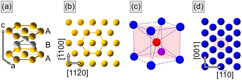
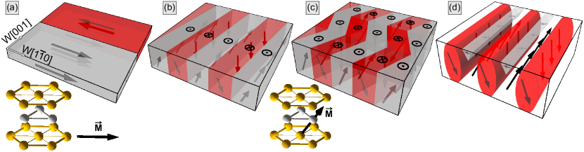
Gd crystallizes in the hexagonal close-packed (hcp) crystal structure with an alternating sequence of A/B/A layers, see Fig. 1(a,b). With a ratio of 1.59, the hcp lattice structure of bulk Gd deviates somewhat from the ideal value, . This causes an anisotropic dipole-dipole interaction which, if considered in isolation, would result in a magnetization pointing along the c-axis. In combination with the above-mentioned small magneto-crystalline anisotropy, it results in an easy axis which—at low temperatures relevant for this study—is rotated by about away from the c-axis Corner and Tanner (1975).
The magnetic properties of Gd thin films epitaxially grown on the (110) surface of refractory body-centered cubic (bcc) W single-crystals have been investigated in numerous studies. The epitaxial growth relation beweeen these two materials is Gd(0001) W(110) and Weller and Alvarado (1986). It was recognized at an early stage that both the film thickness Farle et al. (1993a) and the annealing temperature Stetter et al. (1992); Tober et al. (1996) significantly affect the magnetic properties. The observed enhancement of the ac susceptibility was interpreted in terms of misfit dislocations which are annealed at elevated temperature, whereby the temperature required to optimize the height and width of the peak increased with increasing film thickness Stetter et al. (1992).
Susceptibility measurements also resulted in the identification of a spin reorientation transition (SRT) from in-plane at low film thickness to out-of-plane magnetized stripe domains for Pang et al. (1994); Berger et al. (1994, 1995). This transition was explained with the competition of two energy contributions, i.e., the stray field or magneto-static energy and the uniaxial magneto-crystalline anisotropy energy. Whereas the former dominates for thin films, the latter becomes more relevant for thick films and leads to a rotation of the magnetization towards the c-axis, i.e., perpendicular to the surface plane of Gd(0001)/W(110) Berger et al. (1994, 1995).
A lively discussion developed around the question whether or not the topmost surface layer of Gd(0001) films on W(110) possesses extraordinary magnetic properties, such as an enhanced surface Curie temperature Weller et al. (1985); Tang et al. (1993) or an imperfect or even antiferromagnetic coupling to the bulk Mulhollan et al. (1992); Li et al. (1993). In this context a spin-split –like surface state of Gd(0001) was intensively investigated Li et al. (1994); Weschke et al. (1996); Fedorov et al. (1998); Getzlaff et al. (1998); Bode et al. (1999), essentially rebutting any surface-related magnetic anomaly. The well-defined spin polarization of the occupied majority and the unoccupied minority part of this surface state was later used to establish the spectroscopic mode of spin-polarized scanning tunneling microscopy (SP-STM) Bode et al. (1998); Wiesendanger et al. (1999).
Here we report on a systematic SP-STM investigation of the film thickness-dependent magnetic domain structure of Gd(0001) films epitaxially grown on W(110). To identify optimal growth conditions both the substrate temperature during Gd deposition and the post-deposition annealing temperature were modified. We find that room temperature deposition results in the smoothest films with the lowest density of surface defects, such as step edges, screw and edge dislocations. Spin-resolved measurements clearly show that annealing Gd films at a temperature of 600 K is insufficient to release stacking faults from the as-grown films, resulting in relatively small domains, probably due to domain wall pinning. Only upon annealing to 900 K large domains with straight domain walls were observed. A coverage-dependent SP-STM study of Gd/W(110) in the coverage range between 20 AL and 600 AL finds a spin-reorientation transitions (SRT) from in-plane to out-of-plane at a critical coverage AL, in excellent agreement with earlier findings based on susceptibility measurements Berger et al. (1994, 1995). Stripe domains are imaged for . The high spatial resolution of SP-STM allows for an investigation of the stripe periodicity. While we find that the magnetic stripe domains are homogeneously tilted by either or with respect to the W direction just above , a zig-zag pattern with an alternating stripe orientation is found between 200 AL and 375 AL. In the same coverage regime we find evidence for the formation of branching domains. At even higher Gd coverage irregular stripe domains are found. The observed magnetic domain structures are discussed in terms of competing effects, i.e., the magneto-crystalline, magneto-static, and magneto-elastic contributions to the total energy.
II Experimental setup and procedures
The experiments were performed in a two-chamber ultra-high vacuum (UHV) system with a base pressure . A preparation chamber facilitates tip and sample preparation by electron beam heating to temperatures well above 2300 K. Variable leak valves allow for the dosing of high-purity gases. The single crystal was initially cleaned in an oxygen atmosphere by a two-step-flashing procedure with consecutive low-temperature ( K) and high-temperature ( K) flashes Zakeri et al. (2010). Flash temperatures were measured with an optical pyrometer (Ircon Ultimax UX-20P) at an emissivity and an estimated accuracy of K. The cleanliness of the substrate was confirmed by a sharp low-energy electron diffraction (LEED) pattern with a low background intensity, as will be shown further below, and by scanning tunneling microscopy (STM).
Distilled Gd lumps (MaTeck, purity ) were melted in a Mo crucible and deposited by electron-beam evaporation. The absolute deposition rate is determined to atomic layers (AL) per minute Sup , where the error margin corresponds to a statistical uncertainty due to the limited scan range of our STM images. Therefore, we expect a much lower relative error between samples with different Gd coverage, as they are achieved by a simple scaling of the deposition time. During deposition and LEED experiments, the sample was clamped to a manipulator which can either be cooled by liquid nitrogen, resulting in a sample temperature , or heated by a filament (). On the manipulator the sample temperature is measured by a thermocouple attached to one side of the sample slot. Comparison of temperature readings taken with the optical pyrometer and the thermocouple in the temperature range between 590 K and 890 K agree within K.
Upon preparation, the samples were transferred into the STM chamber. This chamber includes a cryostat cooled with liquid helium which houses a home-built low-temperature STM. It is operated at a base temperature . Measurements were performed with electro-chemically etched W tips. All images were taken in the constant-current mode with the bias voltage applied to the sample. Tunneling d/d spectra and maps were obtained by modulating the bias voltage at a frequency kHz, i.e., well above the cut-off frequency of the feedback loop, and detecting the resulting amplitude of the current modulation with a lock-in amplifier. Typical amplitudes of the bias voltage modulation were mV.
For magnetically sensitive spin-polarized STM measurements, the tip was dipped several nanometers into the Gd surface or gently pulsed at voltages . As stated in more detail in Sec. III.3, this preparation procedure reliably resulted in probe tips which gave a strong tunneling magneto-resistance (TMR) contrast in differential conductivity d/d images, especially around mV. Furthermore, it has the advantage that it comes with a much lower experimental effort than the preparation of thin film tips described in earlier publications Bode (2003), which required a high-temperature treatment and subsequent film deposition and annealing. At the same time, however, it has the disadvantage that the tip magnetization direction is probably not aligned along the in-plane or out-of-plane direction but canted relative to the sample surface. For thin film tips, in contrast, the magnetization direction can be predicted with reasonable confidenceBode (2003) and verified by scanning suitable test samples, for an example see Fig. S3 in Ref. Schmitt et al., 2019. Our preference for a swift magnetic tip preparation technique rather than a much slower method with a more reliable quantization axis is a consequence of the focus of this study, which is on the systematic investigation of a broad variety of preparation parameters, such as the substrate temperature during film deposition, the post-growth annealing temperature, and the Gd film thickness. The sheer number of experimental runs excluded alternative tip preparation procedures. As a result, the easy axis of the domain or the magnetic orientation of domain walls cannot be deduced directly from our SP-STM results. Instead, our interpretation also relies on comparison with published results obtained with spatially averaging experimental techniquesWeller and Alvarado (1986); Berger et al. (1994) and the comparison with domain pattern observed on sample systems other than Gd. Furthermore, the rather large amount of magnetic material in Fe-coated tips often led to a modification of the Gd domain patterns, as observed previously with other sample systems Kubetzka et al. (2002). Our experience shows that magnetic tips prepared by dipping into the Gd film are much less invasive, probably because the effective amount of material is much smaller.
For better visibility of our STM data, the -signal recorded in the topographic constant-current image was augmented by its derivative with respect to the fast scan direction, dd. This image processing suggests to the observer a topography image that is illuminated by an invisible light source from the left. Depending on the maximal corrugation, the exact mixing ratio of and dd varies for different images of this study. As a result, the color-code cannot directly be interpreted as a height information. Wherever necessary, line profiles will be presented to allow for a quantitative assessment. Details of the STM image processing can be found in the supplementary material Sup .
III Results
III.1 Structural properties
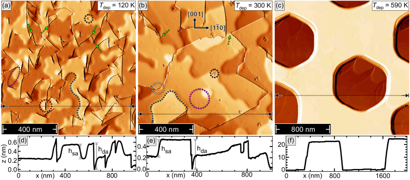
Deposition temperature — In the literature the effect of the W(110) substrate temperature on the Gd film quality has been discussed to some extent. While the majority of studies Aspelmeier et al. (1994); Getzlaff et al. (1999); Bode et al. (1998); Getzlaff et al. (1999, 1998); Bode et al. (1999, 1998); Paschen et al. (1993); Stetter et al. (1992) deposit at about 300 K, some report on enhanced Tober et al. (1996); Mulhollan et al. (1992); Weller and Alvarado (1986) or reduced temperatures Starke (1997). In order to identify the optimal growth conditions for later magnetic domain studies, we deposited Gd films with a thickness of AL onto the W(110) substrate held at various temperatures. Fig. 2 shows STM overviews of samples grown at (a) K, (b) K, and (c) K. Upon film growth, all samples were post-annealed on an e-beam stage at for five minutes. Height profiles measured along the black transparent lines marked in (a)-(c) are presented in Fig. 2(d)-(e), respectively.
The STM topography image of the sample grown at a reduced substrate temperature, Fig. 2(a), is dominated by numerous short step edges which often converge under an acute angle with neighboring step edges, thereby forming a zig-zag pattern of V-shaped single-atomic step edges with double screw dislocations at the joints, exemplary marked by green arrows. The typical length of these step edges is several ten up to a few hundred nanometers and the density of the double screw dislocations amounts to about per .111 Defect densities have been determined on the basis of representative STM images with a scan range of recorded at a pixel resolution. Since the number of events measured within the randomly chosen sampling area follows a Poisson distribution, the error bar given is based on the standard deviation, . Occasionally, two single-atomic step edges emerge and terminate at the same location and run almost in parallel, thereby forming an isolated pair which closely resembles a double step edge. An example is marked by a red dashed circle. These two features, i.e., step edges with a height in close agreement with a single-atomic ( pm) and double-atomic step edges ( pm), can also be recognized in the line section presented in Fig. 2(d) as sharp transitions. Furthermore, numerous point-like indentations (pink dashed circle) with a density of about per , and smoothed-out step edges (grey dashed line) can be recognized, whose origin will be explained later on. We would like to note that a few sharply delimited holes with an apparent depth of about pm can be recognized, one of which is marked by a brown dashed circle. It has been shown in previous studies that these holes are caused by the local adsorption of hydrogen, resulting in the quenching of the -like Gd(0001) surface state Getzlaff et al. (1999). These holes cover less than 0.1% of the total surface area, thereby corroborating the excellent cleanliness of the surface.
The sample prepared at room temperature, Fig. 2(b), exhibits a much lower density of these structural features and, therefore, the overall surface morphology appears much smoother. For example, the density of the V-shaped single-step edges is reduced to about per , i.e., a reduction of about 82% as compared to the low-temperature grown film presented in Fig. 2(a). A similar reduction is also identified for the point-like indentations (pink dashed circle) to about per , which is about 41 % less than for the cold evaporation. The density of smoothed step edges (indicated by a grey dashed line) is also reduced by a similar percentage. The height profile presented in Fig. 2(e) confirms these observations.
The Gd film grown at K shows a completely different surface morphology, see Fig. 2(c). Here we find large hexagonal vacancy islands with depths nm and typical side lengths of about 400 nm [see also the line profile in Fig. 2(f)]. Obviously, the film thickness is no longer homogeneous but at the edge to island formation, in general agreement with similar observations made for thinner films Tober et al. (1996).
These results indicate that the optimal substrate temperature for obtaining homogeneous Gd films with a minimal density of structural defects is K. In contrast, elevated or lowered temperatures result in surface textures with more structural defects which potentially act as pinning centers for magnetic domain walls and are, therefore, unsuitable for imaging the intrinsic domain structure of Gd/W(110) films. A similar behavior with respect to the annealing temperature will be presented in Sec. III.3 below.
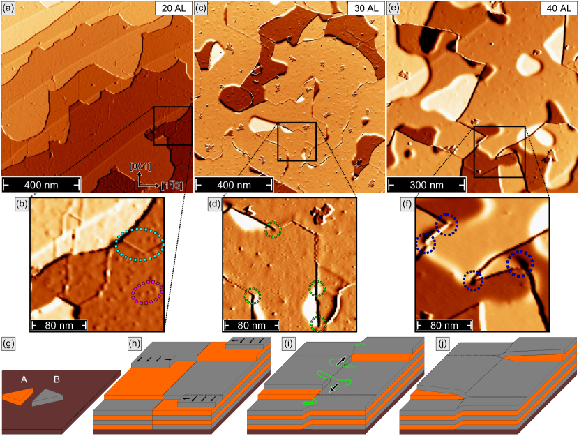
Growth — Figure 3 summarizes the main processes important to understand the structural features of Gd(0001) films grown on W(110). All samples were deposited at room temperature and post-annealed at K for 5 min. Fig. 3(a) shows an overview of the terrace-and-step structure of a 20 AL film. The overgrown step edges of the underlying W substrate can clearly be identified. The zoom-in image reveals that the terraces are not perfectly flat but exhibit trenches which are about pm deep. One example is marked by a cyan circle in Fig. 3(b). Furthermore, numerous point-like indentations (pink circle) can be recognized.
When increasing the film thickness to 30 AL, Fig. 3(c), the film texture changes considerably, as the trenches become deeper (up to 170 – 240 pm). Furthermore, they are more asymmetric and—in some segments—have even converted into full-fledged step edges. Some positions where the transition from an asymmetric trench into a step edge is observed, are marked by green dashed circles in the higher magnification image presented in Fig. 3(d). This transition not only results in a screw dislocation, but also in the appearance of smoothed-out step edges which appear as white bumps in Fig. 3(d). At an even higher film thickness of 40 AL, see Fig. 3(e), the surface morphology is dominated by smoothed steps and double-screw dislocations, some of which are marked by blue dashed circles in the zoom-in in Fig. 3(f). These features have completely replaced the trenches observed at lower coverage, which no longer can be found.
Overall, the thickness-dependent changes observed in Fig. 3(a)-(e) for Gd/W(110) show close resemblance to earlier results of Dy films grown on W(110) reported by Krause et al Krause et al. (2006). In this report it was shown by atomic resolution data that point-like indentations similar to those we observed in Figs. 2(a) and 3(b) are caused by edge dislocations, i.e., an additional semi-infinite plane which releases misfit-related strain. Furthermore, Krause and co-authors proposed a general model Krause et al. (2006), which is reproduced in Fig. 3(g)-(j), that describes the evolution of the rare-earth metal (REM) film morphology on bcc(110) surfaces. The first atomic layer of heavy REMs epitaxially grown on W(110) single crystals reveals a heavily distorted hexagonal lattice Kołaczkiewicz and Bauer (1986); Weller and Alvarado (1986). The nucleation of A- and B-stacked islands, schematically represented in Fig. 3(g), starts with the second atomic layer Getzlaff et al. (1998). These islands grow to patches which maintain their respective stacking order, i.e., A/B/A or B/A/B, even after coalescence when a continuous film is formed at relatively low coverage. As indicated by the differently colored surface layers in Fig. 3(h), however, the film is not translation invariant at the grain boundary between two of these patches, resulting in structural domain boundaries which we observe as trenches in Fig. 3(a) and (b).
Since the energy associated with the grain boundary increases with increasing film thickness, relaxation processes set in at a critical thickness, Fig. 3(i). They lead to so-called partial screw dislocations which shift differently stacked patches by half a lattice constant along the c-axis, i.e., perpendicular to the film plane, and result in a film with continuous A- and B-stacked layers. However, this process is accompanied by a significant surface buckling which in our data appears as smoothed-out step edges, cf. Figs. 2(a), (b) and 3(d). Obviously, for Gd films on W(110) this process starts at a coverage somewhere between 20 and 30 AL. As indicated by black arrows in Fig. 3(i), these partial screw dislocations move with increasing film thickness until an adjacent pair merges, see Fig. 3(j). In this case, their fate depends on the relative orientation of their respective Burgers vectors, . If the two Burgers vectors point in the same direction, a double screw dislocation with its characteristic V-shaped step structure will emerge at the sample surface, cf. Fig. 3(e,f) for a 40 AL film. In contrast, if the two Burgers vectors have opposite signs, the partial screw dislocations will annihilate and form an extended smoothed step edge. This appearance remains qualitatively unchanged up to the thickest Gd films studied here, i.e., 600 AL.
III.2 Electronic Properties
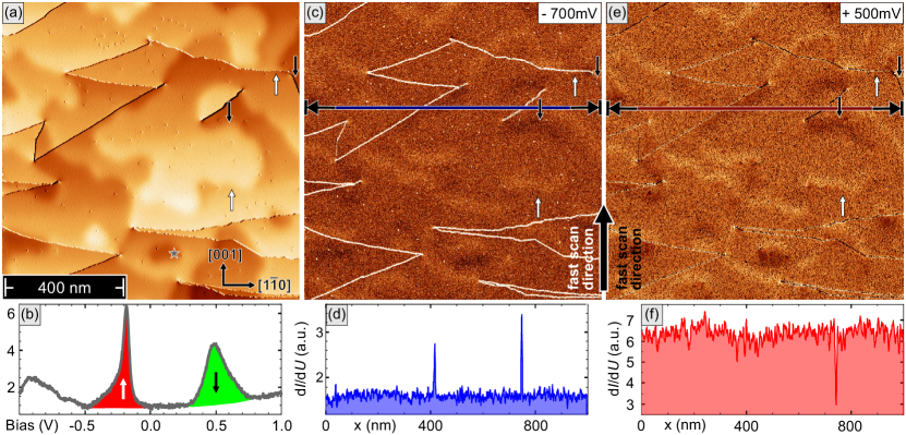
Figure 4 summarizes spin-averaged STM measurements for a 200 AL thick Gd(0001)/W(110) film taken with an unpolarized W tip (see supporting information in Ref. Sup, ). The film was prepared by room temperature deposition and post-growth annealing at for 5 min. In agreement with the data presented so far, the STM topography image shown in Fig. 4(a) exhibits a surface morphology with characteristic double-screw dislocations and smoothed step edges. At the location marked with a grey star in Fig. 4(a), a d/d point spectrum was taken which is plotted in Fig. 4(b). It shows two pronounced peaks which originate from the well-known exchange-split -like surface states of Gd(0001). The occupied majority part appears at a binding energy of meV, whereas the empty minority part is observed at meV, highlighted in red and green in Fig. 4(b), respectively. These values are in good agreement with the binding energies reported in earlier STS studies Bode et al. (1998, 1999); Wegner et al. (2006) and in a combined angle-resolved photoemission (PE) and inverse PE study by Weschke et al Weschke et al. (1996).
Figure 4(c,e) shows d/d maps which were simultaneously obtained at bias voltages (c) mV and (e) mV. As evidenced by the respective slightly smoothed line profiles, presented in Fig. 4(d) and (f) below, in both cases the d/d signal strength shows a relatively small variation, indicating an almost constant density of states (DOS) if measured with a non-magnetic probe tip. The only exceptions are a weak modulation which occurs on length scales of about 100 nm and more narrow dips/peaks. Correlation with the topography image in Fig. 4(a) reveals that these variations of the d/d signal are not related to the local electronic properties of the Gd film, but instead caused by the finite response time of the feedback circuit. A thick arrow between panels (c) and (e) indicates the fast scan direction of these data sets. Obviously, when scanning the tip over smoothed step edges or step edges, such as those marked by arrows in Fig. 4(a), the tip needs to be retracted whenever the sample height increases (upward slope, white arrows) and extended if the sample height decreases (downward slope, black arrows). Due to the finite response time of the feedback circuit this results in a subtle increase or decrease of the tunneling current , respectively. Comparison of the topography in Fig. 4(a) with the d/d maps presented in panels (c) and (e) reveals that this variation of the results in a d/d signal which is enhanced at every upward slope and reduced at downward slopes. The backward scan (opposite fast scan direction, not shown here) exhibits the opposite trend. Therefore, we can conclude that the spin-averaged density of states of the surface of Gd films grown on W(110) as measured with non-magnetic probe tips is essentially homogeneous. As we will see below, this changes if magnetic probe tips are used and enables the imaging of magnetic domains.
III.3 Magnetic Properties
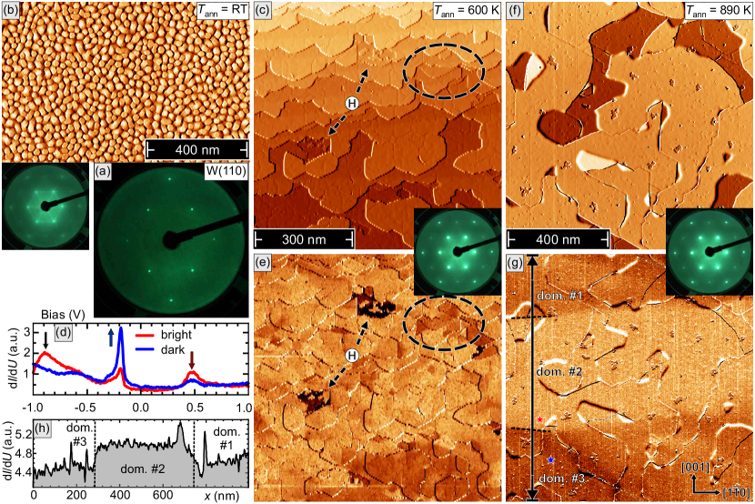
Post-growth annealing temperature — It has been shown in numerous reports that the annealing temperature significantly affects the magnetic properties of Gd(0001) films grown on W(110) substrates Stetter et al. (1992); Pang et al. (1994); Berger et al. (1995); Tober et al. (1996). For example, 50 nm thick films showed a reduced low-temperature coercivity if annealed at K, an effect which was attributed to the annealing of defects Berger et al. (1995). It was argued that “the domain wall mobility is enhanced with improving crystal quality”, thereby resulting “in a reduction of the coercive field” Berger et al. (1995). However, it has also been shown that too high annealing temperatures may result in discontinuous films Stetter et al. (1992); Farle et al. (1993b); Farle and Lewis (1994); Tober et al. (1996).
In order to appropriately evaluate the effects the annealing temperature has on both the surface morphology and the magnetic domain structure, we exemplarily performed a combined LEED and SP-STM study of 30 AL Gd/W(110), see Fig. 5. Fig. 5(a) displays the LEED pattern of clean W(110). As shown in the STM image of Fig. 5(b), Gd deposition without any further annealing results in a very rough surface with numerous hexagon-shaped islands with a typical diameter of 20 nm and several nanometer deep trenches. Similar to earlier reports Stetter et al. (1992), the corresponding LEED pattern, which is shown as an inset in Fig. 5(b), exhibits diffuse refraction spots, most likely resulting from poor long-range order.
Figure 5(c) shows an STM image of a Gd film which was post-annealed at K for 15 minutes. The surface topography is comparable to the data presented in Fig. 3(a) further above. We recognize a decent terrace-and-step growth without any screw dislocations. However, the terraces are not flat but exhibit a large number of line defects, as already discussed in Sec. III.1, indicating a high density of grain boundaries between differently stacked patches of the film. The LEED pattern displayed in the inset shows sharp refraction spots, thereby confirming a much improved crystallinity as compared to the as-grown film presented in Fig. 5(b).
Typical d/d spectra obtained with a spin-polarized Gd/W tip on two locations of a Gd/W(110) film are shown in Fig. 5(d). The locations were chosen somewhat arbitrarily such that the spectra show maximum contrast. We recognize two spectra which are very similar qualitatively, i.e., if solely judged on the basis of the general spectral shape and the peak positions, but which—at least at some bias voltages—differ quite significantly in terms of the d/d signal strength. In close accordance with the spin polarization of Gd(0001) determined by spin-resolved inverse photoemission spectroscopy Donath et al. (1996) and previously published SP-STS results obtained with Fe-coated probe tips Bode et al. (1998); Wiesendanger et al. (1999), we find a contrast reversal between the occupied majority [marked in Fig. 5(d)] and the unoccupied minority part () which takes place at a bias voltage mV. However, with the Gd tips employed here, we find an additional contrast reversal in the occupied states at mV. It appears to be related to a peak which is located at around mV, see black arrow in Fig. 5(d). We tentatively attribute this feature in our STS data to a bundle of Gd bands which originate from hybridizing majority - and -derived states and disperse in the direction of the surface Brillouin zone Kurz et al. (2002). As described in Figs. 8 and 9 of Ref. Kurz et al., 2002, these bands can be found in the energy range between 0.5 eV and 1.0 eV below the Fermi level, exhibit a very flat dispersion and, therefore, are expected to result in an appreciable majority DOS in the surface layer. We would like to note that the bias voltage range just below this peak, especially around mV, turned out to be particularly suited for spin-resolved d/d mapping experiments with Gd/W tips, as the magnetic contrast was most reliable and rather stable.
The spin-dependent contrasts identified in Fig. 5(d) can be utilized to map the magnetic domain structure of the Gd(0001) surface. Fig 5(e) presents a spin-resolved d/d map which was obtained with a magnetically sensitive Gd/W tip simultaneously with the topographic image of Fig. 5(c). The contrast variation here is caused by spin-polarized tunneling and reflects the domain structure of the film.222 Note that the much darker patches (marked by arrows) are caused by the local adsorption of hydrogen Getzlaff et al. (1999). This signal does not contain any magnetic information but only indicates the quenching of the Gd surface state. The magnetic domains visible in Fig. 5(e) are quite irregular, e.g. in the region marked by hatched black ellipses, and often form tiny patches. We speculate that this domain structure is the result of the pinning of magnetic domain walls at structural defects, such as step edges or structural grain boundaries.
As evidenced by the data presented in Fig. 5(f) and (g), annealing of the films profoundly changes the magnetic domain structure of Gd films on W(110). Again, a 30 AL thick Gd film was deposited at room temperature, but the post-annealing temperature is increased to K for 15 min. In comparison to Fig. 5(c), the topographic STM image shown in Fig. 5(f) reveals a much improved surface quality with a strongly reduced density of step edges and structural grain boundaries. At the same time, the LEED pattern (inset) is basically undistinguishable from the one presented in Fig. 5(c), indicating that the short-range crystalline order on length scales of the coherence length of low-energy electrons ( nm) remains unchanged. Although this annealing results in the formation of double-screw dislocations, as described before in Fig. 3, the magnetic domain structure changes considerably, as can be seen in the spin-sensitive d/d map shown in Fig. 5(g). On a scan range we recognize only three magnetic domains, marked as dom. #1 through dom. #3, which are separated by domain walls (highlighted by hatched lines) roughly oriented along the W direction. A line profile of the d/d signal along the arrow across the three domains is plotted in Fig. 5(h). In contrast to the essentially flat data taken with non-magnetic tips, cf. Fig. 4(d) and (f), the line profile presented here features two contrast levels. While a lower d/d signal is recorded at domains #1 and #3, a higher signal is measured for domain #2. Obviously, the reduced density and different kind of structural defects upon annealing to 890 K leads to a strong reduction of the pinning potential for magnetic domain walls. As a result, the film is able to adapt a more uniform domain structure.
Although we are not able to unambiguously determine whether the magnetic domain structures imaged in Fig. 5(g) represents an in-plane or an out-of-plane contrast, we interpret the strongly anisotropic course of the domains walls along the W direction as evidence for a magnetization which is oriented in-plane along this direction. Thereby, the magneto-static energy associated with head-to-head or tail-to-tail spin configurations can be avoided. Unfortunately, a comparison of these data with previous experimental results is in many cases complicated by an insufficient documentation of the scattering geometry. One of the few exceptions is the study of Weller et al., Weller and Alvarado (1986) where it is explicitly stated that their spin-polarized low-energy electron diffraction (SPLEED) experiments are essentially sensitive to a magnetization along the W direction, in agreement with our hypothesis above.
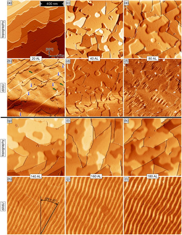
Film thickness-dependent domain structure — We have performed an extensive SP-STM investigation of the thickness-dependent magnetic domain structures of Gd films grown on W(110). As described before, the films were deposited at room temperature and subsequently annealed at K for five minutes on an electron-beam heating stage. We would like to note that a large part of the data presented in Figs. 6 and 7 have been obtained in a relatively short experimental run with the identical tip for which we can exclude even minor tip changes, see Ref. Note, 3. The complete set of data consists of 12 different coverages. The first, low-coverage part of this study is presented in Fig. 6. The six data sets displayed are arranged in two rows divided by a horizontal black line. Each row is subdivided into three columns which show the STM topography in the top and the corresponding, simultaneously measured magnetic d/d map in the bottom image. All images show a scanned area of .
Starting at 20 AL, the Gd film thickness is still below the onset where relaxation processes set in, cf. Fig. 3(h). Correspondingly, the topographic image in Fig. 6(a) exhibits flat terraces separated by single-atomic step edges. On the terraces numerous trenches can be recognized which are characteristic for the structural grain boundaries between differently stacked patches. Yet, as can be seen in the magnetically sensitive d/d map of Fig. 6(b), due to the high annealing temperature their density is sufficiently reduced to allow for large domains. Domain walls are roughly oriented along the W direction. Within individual domains a weak spatial variation of the d/d signal can be recognized. For example, the bright domain which covers more than the upper half of the image, exhibits areas with a slightly enhanced or reduced d/d signal. Comparison of the structural and magnetic data displayed in Fig. 6(a) and (b), respectively, reveals that the modification of the magnetic d/d signal correlates with the orientation of the structural grain boundaries which separate differently stacked patches of the film, cf. Fig. 3(c). Due to the hexagonal symmetry of the Gd surface layer, the structural grain boundaries come in three orientations, marked by blue, red, and green arrows in Fig. 6(b). We speculate that the grain boundaries are accompanied by an additional in-plane anisotropy term which causes the magnetization to locally deviate from the W direction. This deviation leads to an improved or poorer alignment with the tip magnetization, resulting in an enhanced or reduced d/d signal due to the TMR effect, respectively. In Fig. 6(b) regions with grain boundaries oriented along (blue arrows) appear brighter, whereas a darker contrast is observed in regions where they are oriented along (green) or (red). It appears that these dislocation-induced deviations of the magnetization are also responsible for some if not all fluctuations of the domain wall orientation.
Inspection of the STM image of a 40 AL film, displayed in Fig. 6(c), reveals that the structure of the film has changed considerably. The presence of numerous double-screw dislocations and smooth step edges evidences that the film thickness is above the threshold for the relaxation, cf. Fig. 3(i). Nevertheless, the domain structure represented in Fig. 6(d) is essentially the same as for the 20 AL film of Fig. 6(a,b), as it still shows a few extended domains with domain walls along the W direction.
When increasing the Gd coverage further to 80 AL up to 180 AL the structural properties of the surface as imaged by STM remain largely unchanged, see Fig. 6(e,g,i,k). In either case the topography of the surface is dominated by double-screw dislocations, smoothed step edges, and numerous point-like defects indicating the presence of edge dislocations. Yet, the magnetic domain structure changes considerably. For a Gd coverage of 80 AL, Fig. 6(f), we observe several triangle- or lens-shaped areas which exhibit a stripe pattern, whereas the surrounding surface still shows a homogeneous d/d signal. The lateral size of the striped areas typically amounts to a few hundred nanometers. When performing several experimental runs we found this inhomogeneous surface magnetic structure at nominal coverages of AL. We speculate that the variation originates from slight fluctuations of the growth parameters which are beyond our control.
At even higher coverage, between 140 AL and 180 AL, Fig. 6(h,j,l), pronounced periodic stripes cover the entire sample surface. As exemplarily indicated in Fig. 6(h), these stripes are initially tilted by about with respect to the direction of the W substrate. We would like to note that negative tilt angles also occurred, as exemplarily shown in Fig. S4(b) of the Ref. Sup, . Already a superficial inspection suggests that the periodicity of these stripes increases with coverage. Furthermore, an increasing tendency towards orientational deviations from straight stripes becomes manifest. The data presented in Fig. 6(j,l) suggest that the dark stripes are broader than the bright stripes. Close inspection reveals that for these 160 AL and 180 AL thick films a faint intermediate intensity is visible within the dark regions. As will be pointed out below these effects become more pronounced for even thicker films.
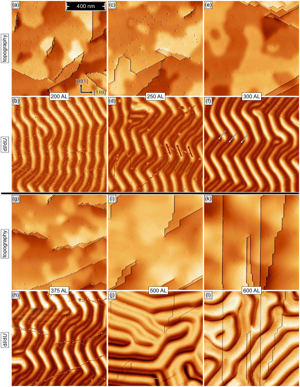
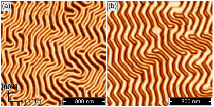
These impressions are further substantiated by the data taken on Gd films with higher coverages which are presented in Fig. 7. For Gd coverages between 200 AL, Fig. 7(a,b), up to 375 AL, Fig. 7(g,h) the stripe orientation more or less periodically switches between positive and negative tilt angles, resulting in an apparent zig-zag like domain pattern. Furthermore, the brightness of the stripes which are tilted by positive and negative angles, becomes increasingly different. These data clearly reveal that the magnetic d/d signal for some stripes no longer oscillates between a minimal and maximal value but exhibits intermediate maxima. Faint bright lines, three of which are marked by white arrows in Fig. 7(f), become visible within the dark segments of the stripes which are rotated in the clockwise direction. These observations will be discussed in the following Sec. IV in detail.
Finally, for very thick films with a Gd coverage of 500 AL, Fig. 7(i), or even 600 AL, Fig. 7(k), the surface topography becomes more and more smooth with fewer and fewer double-screw dislocations, step edges, and edge dislocations. This change in film structure is accompanied by a magnetic domain structure where the domains and domain walls no longer follow certain crystallographic directions, but instead wind quite irregular around one another, see Fig. 7(j,k). Nevertheless, in close similarity to the dark segments observed for the clockwise-rotated stripes in the magnetically sensitive d/d maps of Fig. 7(b,d,f,h), the stripe pattern displays intermediate minima and maxima of the d/d signal in the bright and dark stripes, respectively.
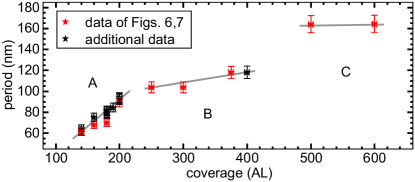
Figure 8 summarizes the periodicities of the stripe domains extracted from Figs. 6 and 7 for Gd film thicknesses between 140 AL and 500 AL. We can recognize three coverage ranges, labelled A–C in Fig. 8. A linear increase is obtained in A, where the periodicity increases from nm at a 140 AL up to nm for a 200 AL thick Gd film. For even thicker Gd films, i.e. in the thickness range B between 200 AL AL, the periodicity increase seems to level off until another increase occurs towards C between 400 AL AL.
IV Discussion
The data presented in Figs. 6 and 7 can be explained qualitatively by the subtle interplay between the exchange energy, the magneto-static energy related to the stray field, and magneto-crystalline contributions to the anisotropy. For Gd/W(110) these magnetic properties are—in comparison to bulk Gd—strongly modified by the presence of substantial epitaxial strain. For thin films up to about 60 AL we find rather large domains, cf. Figs. 5(g) and 6(b,d). SP-STM images with a scan range of typically show 1-2 domain walls only, roughly oriented along the W direction.
As sketched in Fig. 9(a), this observation is consistent with films magnetized along this in-plane axis. It appears that—even though the easy axis of bulk Gd is tilted by from the c-axis—a perpendicular or canted magnetization relative to the sample plane is energetically unfavorable for thin films. This could either be caused by (i) the relatively large magneto-static energy associated with any significant out-of-plane magnetization, or (ii) by the uniaxial strain of the hexagonal Gd(0001) lattice due to epitaxial growth on the rectangular W(110) unit cell (see Fig. 1) which might modify the magneto-crystalline anisotropy energy density. Also a combination of the two effects cannot be excluded.
As the film thickness exceeds a critical value AL, a spin reorientation transition (SRT) from in-plane to out-of-plane is observed. While we are unable to identify the exact physical origin of the SRT in Gd/W(110), it is obvious that, at this coverage, it becomes energetically unfavorable to align the magnetization with the film plane. If the magneto-static energy was responsible for the in-plane magnetization [scenario (i)], the energy penalty related to the film’s magneto-crystalline anisotropy overcompensates this effect for coverages . Likewise (ii), it might be possible that the epitaxial strain relaxes to an extent unsuitable to maintain a magnetization along the in-plane axis.
Upon rotation of the easy axis to out-of-plane, the Gd film forms stripe domains which result in a flux-closure configuration between adjacent domains and thereby reduce the sample’s stray field. Stripe domains in perpendicularly magnetized thin films have frequently been observed and intensively been discussed in the literature. They originate from the competition between exchange interaction which favors a parallel orientation of the spins, and the magneto-static energy associated to the stray field which can be minimized by the formation of antiparallel domains.
Particular attention was paid to the properties of stripe domains in the vicinity of a spin reorientation transition (SRT) where the easy axis of magnetization rotates from out-of-plane to in-plane or vice versa. It has generally been observed on transition metal films with a thickness of a few atomic layers only Speckmann et al. (1995); Oepen et al. (1997); Wu et al. (2004), that the periodicity of the out-of-plane magnetized stripe domains decreases as one approaches the critical thickness of the SRT. Our results presented in Fig. 8 are in qualitative agreement with these results. However, in ultra-thin film systems—irrespective whether the SRT occurs from out-of-plane at low film thickness to in-plane for thick films or vice versa—the stripe density usually increases exponentially as one approaches the SRT Wu et al. (2004); Won et al. (2005). In contrast, for Gd films on W(110) we find a stripe periodicity which increases linearly with film thickness from just above AL up to about 200 AL, cf. Fig. 8.
An analogous SRT with a critical film thickness of 27 nm and a linearly increasing stripe width has been found for FePd films Gehanno et al. (1999). The different behavior was assigned to the fact that the FePd films were much thicker than the ultra-thin films mentioned above. While the spins in ultra-thin films can be considered as rigidly tightened together in the vertical direction by the exchange interaction, this is not necessarily the case for much thicker films. As a result, the magnetization component normal to the film plane, , can vary with the distance from the interface Gehanno et al. (1999). Although we are not able to present a conclusive picture of how the experimentally observed domain periodicities can be explained, we speculate that the major qualitative changes of the magnetic pattern from stripe domains to zig-zag stripe domains and branching domains might also be responsible for the reduced slope of the periodicity increase for Gd films with AL as well as for the further increase at 400 AL AL.
Interestingly, when reaching the critical film thickness AL, we could image indications for an inhomogeneous nucleation of stripe domains, cf. Fig. 6(f). Although we cannot strictly exclude that the weak stray field of the Gd/W tip influences these nucleation processes Kubetzka et al. (2002, 2003), our data are in good qualitative agreement with earlier photoemission electron microscopy (PEEM) experiments, where the local melting of stripe domains was observed, thereby giving rise to paramagnetic patches Won et al. (2005).
At coverages , the data of Fig. 6(h,j,l) and Fig. 7(b,d,f,h) showed stripe domains which were not oriented along a low-index in-plane axis of the W(110) substrate, but rotated within the film plane by about with respect to the W direction. At the same time we know from literature that the bulk easy magnetization direction of Gd is tilted by relative to the c-axis. Both conditions can be approximately fulfilled simultaneously by a magnetization which is, for example, oriented along the Gd direction, indicated by a black arrow in the inset of Fig. 9(b).
This vector includes an angle of with respect to the c-axis and its projection onto the (0001) surface is tilted by to the W and the Gd direction. The resulting magnetic domain structure which is schematically represented in the sketch of Fig. 9(b) is in very good agreement with the conclusions drawn by Berger and co-workers based on susceptibility measurements Pang et al. (1994); Berger et al. (1994, 1995). Also the critical film thickness AL identified by us agrees reasonably well with the value of 40 nm determined by Berger and co-workers, which corresponds to 138 AL Berger et al. (1994, 1995).
As the film thickness is increased beyond approximately 200 AL, several interesting effects can be observed. Firstly, the stripes are no longer straight. Instead of extended areas with uniformly oriented domains, we find stripes the orientation of which frequently changes between and , thereby forming a zig-zag pattern with a typical distance between turning points of several hundred nanometers. This zig-zag pattern may be related to magneto-elastic interactions caused by the uniaxial strain associated to the growth of Gd on a W(110) crystal surface. Since the crystallographic symmetry of the W(110) surface imposes two mirror lines, i.e., the and the axis, any situation where the domain and domain wall orientation uniformly deviate from these axes would result in a net magneto-elastic strain which is incompatible to the “elastic environment”, see Sec. 3.3.1 in Ref. Hubert, A. and Schäfer, R., 2008. By forming magnetic domains which more or less periodically switch their orientation between and , any global strain away from the above-mentioned axes is avoided.
Secondly, the magnetic contrast observed for stripe domains which are rotated by and with respect to the W direction is strikingly different, cf. Fig. 7(d,f,h). In these data sets—all measured with the same magnetic tip333The identity of the tip apex was confirmed by the comparison of tunneling spectra measured on the surfaces of Fig. 7(d,f,h). Since the energetic position of the –like surface states remains unchanged for Gd films with a local coverage ALGetzlaff et al. (1998), any modification of the recorded d/d spectra could safely be attributed to a tip change. However, the spectra measured on the sample surfaces of Fig. 7(d,f,h) were virtually identical (not shown here), thereby verifying the fact that the tip apex remained unchanged during these experiments.—the (anti)-clockwise rotated domains appear much darker (brighter). Since purely out-of-plane domains would be degenerate with respect to the rotational sense, we conclude that a significant in-plane component also exists. We speculate, that this canted magnetization is the result of a significant magneto-crystalline contribution. As discussed in the context of Fig. 9(b), we expect that the in-plane component of the magnetization is oriented along the or equivalent directions, such that the moments are along the easy axis of bulk Gd and at the same time aligned with the stripes domains. The schematic representation of the zig-zag domain structure is presented in Fig. 9(c).
Thirdly, the magnetic d/d signal of some domains of Gd films with a thickness between 250 AL and 375 AL no longer oscillates between a minimal and maximal value, as observed for thinner films just above the SRT, but exhibits intermediate maxima, cf. Fig. 7(d,f,h). This finding may be associated with the formation of branching domains, as originally proposed by Lifschitz Lifschitz and Ruderman (1992). The general concept of branching domains is that “a progressive domain refinement towards the surface by iterated generations of domains” results in a “gain in closure energy”, see Sec. 3.7.5 in Ref. Hubert, A. and Schäfer, R., 2008. We interpret the appearance of the intermediate maximum as the first set of branching domains. A potential domain structure with in-plane closure domains is sketched in Fig. 9(d).
We would like to note, however, that the intermediate maxima could initially only be observed in regions where the darker, clockwise rotated domains appear. No indication could be found in the anti-clockwise rotated stripe domains. We can only speculate about the reason for this asymmetry. One explanation would be that (i) branching domains exclusively exist for one stripe orientation, though we were not able to identify a simple explanation of how this directional selectivity might come about. Another explanation is (ii) related to the fact that the Gd/W tip we are using is known to exhibit a significant in-plane component. As we will show by data taken with different tips below, the branching domain increases the magnetic d/d signal in some regions, but has no significant effect in another region.
Finally, for very thick Gd films we observe winding stripe domains which are no longer aligned along a preferred direction. Especially in Fig. 7(j) branching domains can be identified. Interestingly, this now includes both, dark and bright irregular stripe domains which clearly present weaker and rather narrow bright and dark intermediate d/d signals, respectively. This observation suggests that the above-mentioned absence of intermediate maxima along some stripe direction in thinner films was indeed caused by a particular tip magnetization direction unsuitable for resolving these closure domains.
As further evidence for this hypothesis we present the data of Fig. 10 which were obtained on the same 400 AL Gd film. As described in Sec. II, the W tip was initially prepared by poking the tip into the Gd film. This Gd/W tip was then used to measure the magnetically sensitive d/d map presented in Fig. 10(a). Afterwards, the tip was again dipped into the Gd film to modify its quantization axis. This tip was then used to obtain the data of Fig. 10(b). Although the data were measured on the same Gd film and the observed domain structures are quite similar as far as the stripe periodicity and the general appearance are concerned, some details are strikingly different. In particular, we notice that the intermediate contrast can clearly be recognized for the entire data set of Fig. 10(a), i.e., irrespective of the stripe orientation. In contrast, the intermediate contrast can only be found for one stripe direction in Fig. 10(b). These data evidence that the apparent absence of branching domains observed in some images, cf. Fig. 7(d,f,h), is not caused by their factual inexistence, but rather by an unfavorable orientation of the tip magnetization, rendering the observation impossible.
V Summary
In this contribution we presented a detailed spin-polarized scanning tunneling microscopy (SP-STM) study of the epitaxial Gd films grown on a W(110) surface. To the best of our knowledge, our data provide the first high-spatial resolution images of the magnetic domains structure of this rare-earth metal. Great care was taken to identify optimal preparation conditions which produce the lowest density of surface defects. Best results were obtained for room temperature deposition followed by subsequent annealing at 900 K. Whereas lower or higher annealing temperatures led to domain wall pinning or discontinuous films, respectively, optimally prepared Gd films with a thickness of 30 atomic layers (AL) exhibit large in-plane magnetized domains with domain walls which are approximately oriented along the direction of the underlying W substrate. In good agreement with earlier spatially averaging studies Pang et al. (1994); Berger et al. (1994, 1995), we find a spin reorientation transition (SRT) at a critical film thicknesses AL where the easy axis of magnetization rotates from parallel to perpendicular to the film plane. SP-STM images taken in the thickness-regime of the SRT reveal a magnetic domain structure which appears to be spatially inhomogeneous, with patches showing a stripe domain phase that coexist with paramagnetic or in-plane ferromagnetic regions. At the coverages exceeds we find stripe domains which are rotated by with respect to the W direction. The periodicity of the stripe domains is investigated thoroughly. Furthermore, at AL we find a magnetic domains structure which resembles a zig-zag pattern. Irregular stripe domains are imaged beyond 500 AL. Our experimental data can consistently be explained by the interplay between different contribution to the total energy, i.e., the magneto-crystalline, the magneto-static, and the magneto-elastic energy density.
Acknowledgments
This work was supported by the DFG through SFB 1170 (project A02). We also acknowledge financial support by the Deutsche Forschungsgemeinschaft (DFG, German Research Foundation) under Germany’s Excellence Strategy through Würzburg-Dresden Cluster of Excellence on Complexity and Topology in Quantum Matter – ct.qmat (EXC 2147, project-id 390858490).
References
- Ripka and Janosek (2010) P. Ripka and M. Janosek, “Advances in magnetic field sensors,” IEEE Sensors Journal 10, 1108–1116 (2010).
- Bhat (2018) W. A. Bhat, “Is a data-capacity gap inevitable in big data storage?” Computer 51, 54–62 (2018).
- Bader et al. (1986) S. D. Bader, E. R. Moog, and P. Grünberg, “Magnetic hysteresis of epitaxially-deposited iron in the monolayer range: A Kerr effect experiment in surface magnetism,” J. Magn. Magn. Mater. 53, L295–L298 (1986).
- Schumann et al. (2000) F. O. Schumann, R. F. Willis, and J. G. Tobin, “Surface-sensitive, element-specific magnetometry with x-ray linear dichroism,” J. Vac. Sci. & Techn. A 18, 1259–1263 (2000).
- Bode (2003) M. Bode, “Spin-polarized scanning tunnelling microscopy,” Rep. Progr. Phys. 66, 523–582 (2003).
- Schwarz and Wiesendanger (2008) A. Schwarz and R. Wiesendanger, “Magnetic sensitive force microscopy,” nano today 3, 28–39 (2008).
- Rougemaille and Schmid (2010) N. Rougemaille and A. K. Schmid, “Magnetic imaging with spin-polarized low-energy electron microscopy,” Eur. Phys. Jour. Appl. Phys. 50, 20101 (2010).
- McCord (2015) J. McCord, “Progress in magnetic domain observation by advanced magneto-optical microscopy,” Journal of Phys. D: Appl. Phys. 48, 333001 (2015).
- Hauptmann et al. (2017) N. Hauptmann, J. W. Gerritsen, D. Wegner, and A. A. Khajetoorians, “Sensing noncollinear magnetism at the atomic scale combining magnetic exchange and spin-polarized imaging,” Nano Letters 17, 5660–5665 (2017).
- Kohashi (2018) T. Kohashi, “Magnetization analysis by spin-polarized scanning electron microscopy,” Scanning 2018, 2420747 (2018).
- Elmers et al. (1994) H. J. Elmers, J. Hauschild, H. Höche, U. Gradmann, H. Bethge, D. Heuer, and U. Köhler, “Submonolayer Magnetism of Fe(110) on W(110): Finite Width Scaling of Stripes and Percolation between Islands,” Phys. Rev. Lett. 73, 898–901 (1994).
- Mentz et al. (1999) E. Mentz, A. Bauer, T. Günther, and G. Kaindl, “Magnetization reversal and spin reorientation in Fe/Cu(100) ultrathin films,” Phys. Rev. B 60, 7379–7384 (1999).
- Allenspach and Bischof (1992) R. Allenspach and A. Bischof, “Magnetization direction switching in Fe/Cu(100) epitaxial films: Temperature and thickness dependence,” Phys. Rev. Lett. 69, 3385–3388 (1992).
- Thomassen et al. (1992) J. Thomassen, F. May, B. Feldmann, M. Wuttig, and H. Ibach, “Magnetic live surface layers in Fe/Cu(100),” Phys. Rev. Lett. 69, 3831–3834 (1992).
- Wu et al. (2004) Y. Z. Wu, C. Won, A. Scholl, A. Doran, H. W. Zhao, X. F. Jin, and Z. Q. Qiu, “Magnetic stripe domains in coupled magnetic sandwiches,” Phys. Rev. Lett. 93, 117205 (2004).
- Berger et al. (1992) A. Berger, U. Linke, and H. P. Oepen, “Symmetry-induced uniaxial anisotropy in ultrathin epitaxial cobalt films grown on Cu(1 1 13),” Phys. Rev. Lett. 68, 839–842 (1992).
- Kawakami et al. (1996) R. K. Kawakami, Ernesto J. Escorcia-Aparicio, and Z. Q. Qiu, “Symmetry-Induced Magnetic Anisotropy in Fe Films Grown on Stepped Ag(001),” Phys. Rev. Lett. 77, 2570–2573 (1996).
- Bode et al. (2007) M. Bode, M. Heide, K. von Bergmann, P. Ferriani, S. Heinze, G. Bihlmayer, A. Kubetzka, O. Pietzsch, S. Blügel, and R. Wiesendanger, “Chiral magnetic order at surfaces driven by inversion asymmetry,” Nature 447, 190–193 (2007).
- Ferriani et al. (2008) P. Ferriani, K. von Bergmann, E. Y. Vedmedenko, S. Heinze, M. Bode, M. Heide, G. Bihlmayer, S. Blügel, and R. Wiesendanger, “Atomic-Scale Spin Spiral with a Unique Rotational Sense: Mn Monolayer on W(001),” Phys. Rev. Lett. 101, 027201 (2008).
- Heinze et al. (2011) S. Heinze, K. von Bergmann, M. Menzel, J. Brede, A. Kubetzka, R. Wiesendanger, G. Bihlmayer, and S. Blügel, “Spontaneous atomic-scale magnetic skyrmion lattice in two dimensions,” Nature Phys. 7, 713–718 (2011).
- Krause et al. (2006) S. Krause, L. Berbil-Bautista, T. Hänke, F. Vonau, M. Bode, and R. Wiesendanger, “Consequences of line defects on the magnetic structure of high anisotropy films: Pinning centers on Dy/W(110),” Europhys. Lett. (EPL) 76, 637–643 (2006).
- Berbil-Bautista et al. (2007) L. Berbil-Bautista, S. Krause, M. Bode, and R. Wiesendanger, “Spin-polarized scanning tunneling microscopy and spectroscopy of ferromagnetic Dy(0001)/W(110) films,” Phys. Rev. B 76, 064411 (2007).
- Berbil-Bautista et al. (2009) L. Berbil-Bautista, S. Krause, M. Bode, A. Badía-Majós, C. de la Fuente, R. Wiesendanger, and J. I. Arnaudas, “Nanoscale spin structures dominated by magnetoelastic interactions around dislocation cores as seen via spin-polarized STM,” Phys. Rev. B 80, 241408 (2009).
- Prieto et al. (2016) J. E. Prieto, G. Chen, A. K. Schmid, and J. de la Figuera, “Magnetism of epitaxial Tb films on W(110) studied by spin-polarized low-energy electron microscopy,” Phys. Rev. B 94, 174445 (2016).
- Kamber et al. (2020) U. Kamber, A. Bergman, A. Eich, D. Iusan, M. Steinbrecher, N. Hauptmann, L. Nordström, M. I. Katsnelson, D. Wegner, O. Eriksson, and A. A. Khajetoorians, “Self-induced spin glass state in elemental and crystalline neodymium,” Science 368, 966 (2020).
- Getzlaff et al. (1999) M. Getzlaff, M. Bode, R. Pascal, and R. Wiesendanger, “Adsorbates on Gd(0001): A combined scanning tunneling microscopy and photoemission study,” Phys. Rev. B 59, 8195–8208 (1999).
- Wegner et al. (2007) D. Wegner, A. Bauer, and G. Kaindl, “Effect of impurities on tamm-like lanthanide-metal surface states,” Phys. Rev. B 76, 113410 (2007).
- Baberschke et al. (1987) K. Baberschke, M. Farle, and M. Zomack, “The ferromagnetic order and the critical exponent of Gd monolayers and thin films on W(110),” Appl. Phys. A 44, 13–18 (1987).
- Corner and Tanner (1975) W. D. Corner and B. K. Tanner, “The easy direction of magnetization in gadolinium,” J. Phys. C: Sol. State Phys. 9, 627–633 (1975).
- Weller and Alvarado (1986) D. Weller and S. F. Alvarado, “Preparation of remanently ferromagnetic Gd(0001),” J. Appl. Phys. 59, 2908 (1986).
- Farle et al. (1993a) M. Farle, K. Baberschke, U. Stetter, A. Aspelmeier, and F. Gerhardter, “Thickness-dependent Curie temperature of Gd(0001)/W(110) and its dependence on the growth conditions,” Phys. Rev. B 47, 11571–11574 (1993a).
- Stetter et al. (1992) U. Stetter, M. Farle, K. Baberschke, and W. G. Clark, “Critical behavior of strained epitaxial Gd films: In situ ac-susceptibility measurements in UHV,” Phys. Rev. B 45, 503 (1992).
- Tober et al. (1996) E. D. Tober, R. X. Ynzunza, C. Westphal, and C. S. Fadley, “Relationship between morphology and magnetic behavior for Gd thin films on W(110),” Phys. Rev. B 53, 5444–5448 (1996).
- Pang et al. (1994) A. W. Pang, A. Berger, and H. Hopster, “Magnetization behavior of thick epitaxial Gd(0001) films on W(110),” Phys. Rev. B 50, 6457 (1994).
- Berger et al. (1994) A. Berger, A.W. Pang, and H. Hopster, “Magnetic reorientation transition in epitaxial gd-films,” Journal of Magnetism and Magnetic Materials 137, L1–L5 (1994).
- Berger et al. (1995) A. Berger, A. W. Pang, and H. Hopster, “Magnetic reorientation transition of Gd(0001)/W(110) films,” Phys. Rev. B 52, 1078 (1995).
- Weller et al. (1985) D. Weller, S. F. Alvarado, W. Gudat, K. Schröder, and M. Campagna, “Observation of Surface-Enhanced Magnetic Order and Magnetic Surface Reconstruction on Gd(0001),” Phys. Rev. Lett. 54, 1555 (1985).
- Tang et al. (1993) H. Tang, D. Weller, T. G. Walker, J. C. Scott, C. Chappert, H. Hopster, A. W. Pang, D. S. Dessau, and D. P. Pappas, “Magnetic reconstruction of the Gd(0001) surface,” Phys. Rev. Lett. 71, 444–447 (1993).
- Mulhollan et al. (1992) G. A. Mulhollan, K. Garrison, and J. L. Erskine, “Surface magnetism of Gd(0001): Evidence of ferromagnetic coupling to bulk,” Phys. Rev. Lett. 69, 3240–3243 (1992).
- Li et al. (1993) D. Li, J. Zhang, P. A. Dowben, and K. Garrison, “Evidence for imperfect ferromagnetic coupling between the Gd(0001) surface and the bulk,” J. Phys.: Cond. Matter 5, L73–L76 (1993).
- Li et al. (1994) D. Li, P. A. Dowben, J. E. Ortega, and F. J. Himpsel, “Unoccupied surface electronic structure of Gd(0001),” Phys. Rev. B 49, 7734–7738 (1994).
- Weschke et al. (1996) E. Weschke, C. Schüssler-Langeheine, R. Meier, A. V. Fedorov, K. Starke, F. Hübinger, and G. Kaindl, “Temperature Dependence of the Exchange Splitting of the Surface State on Gd(0001): Evidence against Spin-Mixing Behavior,” Phys. Rev. Lett. 77, 3415–3418 (1996).
- Fedorov et al. (1998) A.V. Fedorov, T. Valla, D.J. Huang, G. Reisfeld, F. Loeb, F. Liu, and P.D. Johnson, “Spin polarized photoemission studies of the Gd(0001) surface,” J. Electr. Spectr. Rel. Phenom. 92, 19–24 (1998).
- Getzlaff et al. (1998) M. Getzlaff, M. Bode, S. Heinze, R. Pascal, and R. Wiesendanger, “Temperature-dependent exchange splitting of the magnetic Gd(0001) surface state,” J. Magn. Magn. Mater. 184, 155–165 (1998).
- Bode et al. (1999) M. Bode, M. Getzlaff, A. Kubetzka, R. Pascal, O. Pietzsch, and R. Wiesendanger, “Temperature-dependent exchange splitting of a surface state on a local-moment magnet: Tb(0001),” Phys. Rev. Lett. 83, 3017 (1999).
- Bode et al. (1998) M. Bode, M. Getzlaff, and R. Wiesendanger, “Spin-Polarized Vacuum Tunneling into the Exchange-Split Surface State of Gd(0001),” Phys. Rev. Lett. 81, 4256 (1998).
- Wiesendanger et al. (1999) R. Wiesendanger, M. Bode, and M. Getzlaff, “Vacuum-tunneling magnetoresistance: The role of spin-polarized surface states,” Appl. Phys. Lett. 75, 124–126 (1999).
- Zakeri et al. (2010) Kh. Zakeri, T. R. F. Peixoto, Y. Zhang, J. Prokop, and J. Kirschner, “On the preparation of clean tungsten single crystals,” Surf. Sci. 604, L1–L3 (2010).
- (49) See Supplemental Material at http://link.aps.org/supplemental/XXX for detailed information regarding evaluation of the deposition rate, image processing procedures, preparation of an unpolarized tip and the verification of the stripe domains tilted in the opposite direction.
- Schmitt et al. (2019) M. Schmitt, P. Moras, G. Bihlmayer, R. Cotsakis, M. Vogt, J. Kemmer, A. Belabbes, P. M. Sheverdyaeva, A. K. Kundu, C. Carbone, S. Blügel, and M. Bode, “Indirect chiral magnetic exchange through Dzyaloshinskii-Moriya-enhanced RKKY interactions in manganese oxide chains on Ir(100),” Nature Communications 10, 2610 (2019).
- Kubetzka et al. (2002) A. Kubetzka, M. Bode, O. Pietzsch, and R. Wiesendanger, “Spin-polarized scanning tunneling microscopy with antiferromagnetic probe tips,” Phys. Rev. Lett. 88, 057201 (2002).
- Aspelmeier et al. (1994) A. Aspelmeier, F. Gerhardter, and K. Baberschke, “Magnetism and structure of ultrathin Gd films,” Journ. Magn. Magn. Mater. 132, 22–30 (1994).
- Paschen et al. (1993) U. Paschen, C. Sürgers, and H. v. Löhneysen, “Magnetic properties of thin epitaxial Gd films on Nb,” Z. Phys. B Cond. Matter 90, 289 (1993).
- Starke (1997) Kai Starke, “private communication,” (1997).
- Note (1) Defect densities have been determined on the basis of representative STM images with a scan range of recorded at a pixel resolution. Since the number of events measured within the randomly chosen sampling area follows a Poisson distribution, the error bar given is based on the standard deviation, .
- Kołaczkiewicz and Bauer (1986) J. Kołaczkiewicz and E. Bauer, “The adsorption of Eu, Gd and Tb on the W (110) surface,” Surf. Sci. 175, 487 (1986).
- Wegner et al. (2006) D. Wegner, A. Bauer, and G. Kaindl, “Magnon-broadening of exchange-split surface states on lanthanide metals,” Phys. Rev. B 73, 165415 (2006).
- Farle et al. (1993b) M. Farle, W. A. Lewis, and K. Baberschke, “Detailed analysis of the in situ magneto–optic Kerr signal of gadolinium films near the Curie temperature,” Appl. Phys. Lett. 62, 2728 (1993b).
- Farle and Lewis (1994) M. Farle and W. A. Lewis, “Magnetization of thin Gd films on W(110) near the Curie temperature,” Journal of Applied Physics 75, 5604 (1994).
- Donath et al. (1996) M. Donath, B. Gubanka, and F. Passek, “Temperature-dependent spin polarization of magnetic surface state at Gd(0001),” Phys. Rev. Lett. 77, 5138–5141 (1996).
- Kurz et al. (2002) Ph. Kurz, G. Bihlmayer, and S. Blügel, “Magnetism and electronic structure of hcp Gd and the Gd(0001) surface,” J. Phys.: Cond. Matter 14, 6353–6371 (2002).
- Note (2) Note that the much darker patches (marked by arrows) are caused by the local adsorption of hydrogen Getzlaff et al. (1999). This signal does not contain any magnetic information but only indicates the quenching of the Gd surface state.
- Note (3) The identity of the tip apex was confirmed by the comparison of tunneling spectra measured on the surfaces of Fig.\tmspace+.1667em7(d,f,h). Since the energetic position of the –like surface states remains unchanged for Gd films with a local coverage \tmspace+.1667emALGetzlaff et al. (1998), any modification of the recorded d/d spectra could safely be attributed to a tip change. However, the spectra measured on the sample surfaces of Fig.\tmspace+.1667em7(d,f,h) were virtually identical (not shown here), thereby verifying the fact that the tip apex remained unchanged during these experiments.
- Speckmann et al. (1995) M. Speckmann, H. P. Oepen, and H. Ibach, “Magnetic domain structures in ultrathin Co/Au(111): On the influence of film morphology,” Phys. Rev. Lett. 75, 2035–2038 (1995).
- Oepen et al. (1997) H. P. Oepen, M. Speckmann, Y. Millev, and J. Kirschner, “Unified approach to thickness-driven magnetic reorientation transitions,” Phys. Rev. B 55, 2752–2755 (1997).
- Won et al. (2005) C. Won, Y. Z. Wu, J. Choi, W. Kim, A. Scholl, A. Doran, T. Owens, J. Wu, X. F. Jin, H. W. Zhao, and Z. Q. Qiu, “Magnetic stripe melting at the spin reorientation transition in Fe/Ni/Cu(001),” Phys. Rev. B 71, 224429 (2005).
- Gehanno et al. (1999) V. Gehanno, R. Hoffmann, Y. Samson, A. Marty, and S. Auffret, “In plane to out of plane magnetic reorientation transition in partially ordered FePd thin films,” Eur. Phys. Jour. B–Cond. Mat. Compl. Syst. 10, 457–464 (1999).
- Kubetzka et al. (2003) A. Kubetzka, O. Pietzsch, M. Bode, and R. Wiesendanger, “Spin-polarized scanning tunneling microscopy study of walls in an external magnetic field,” Phys. Rev. B 67, 020401 (2003).
- Hubert, A. and Schäfer, R. (2008) Hubert, A. and Schäfer, R., Magnetic Domains - The Analysis of Magnetic Microstructures (Springer Science and Business Media, Berlin Heidelberg, 2008).
- Lifschitz and Ruderman (1992) E. Lifschitz and E. Ruderman, “On the magnetic structure of iron,” in Persp. Theor. Phys., edited by L. P. Pitaevski (Pergamon, 1992) pp. 203–218.