Asymmetric magnetic proximity interactions in MoSe2/CrBr3 van der Waals heterostructures
Magnetic proximity interactions (MPIs) between atomically-thin semiconductors and two-dimensional magnets provide a means to manipulate spin and valley degrees of freedom in nonmagnetic monolayers, without the use of applied magnetic fields Zutic:2019 ; Gilbertini:2019 ; Mak:2019 . In such van der Waals (vdW) heterostructures, MPIs originate in the nanometer-scale coupling between the spin-dependent electronic wavefunctions in the two materials, and typically their overall effect is regarded as an effective magnetic field acting on the semiconductor monolayer Zhao:NatNano:2017 ; Zhong:SciAdv:2017 ; Norden:NatComm:2019 ; Zhong:NatNano:2020 ; Ciorciaro:PRL:2020 . Here we demonstrate that this picture, while appealing, is incomplete: The effects of MPIs in vdW heterostructures can be markedly asymmetric, in contrast to that from an applied magnetic field. Valley-resolved optical reflection spectroscopy of MoSe2/CrBr3 vdW structures reveals strikingly different energy shifts in the and valleys of the MoSe2, due to ferromagnetism in the CrBr3 layer. Strong asymmetry is observed at both the A- and B-exciton resonances. Density-functional calculations indicate that valley-asymmetric MPIs depend sensitively on the spin-dependent hybridization of overlapping bands, and as such are likely a general feature of such hybrid vdW structures. These studies suggest routes to selectively control specific spin and valley states in monolayer semiconductors Xiao:PRL:2012 ; Xu:2014 .
The ability of short-range proximity interactions to imbue magnetic functionality into otherwise nonmagnetic materials Lazic:2016 ; Kawakami:2018 has exciting prospects for devices that combine the optical and electrical properties of monolayer semiconductors MakShan:2016 ; Urbaszek:2018 ; Strano:2012 with additional tuning parameters that couple directly to spin and valley pseudospin Schaibley:2016 . The atomically-smooth surfaces that are nowadays routinely achieved with van der Waals materials allow for nearly ideal interfaces between monolayer transition-metal dichalcogenide semiconductors (such as WSe2 or MoS2) and magnetic substrates (such as EuO or CrI3). Theoretical studies along these lines Qi:2015 ; Schwingenschlogl:2016 ; Scharf:PRL:2017 ; Zollner:2019 ; Zhang:2019 ; Xie:2019 have been validated by experiments demonstrating, e.g., enhanced valley splitting of WSe2 and WS2 monolayers on ferromagnetic EuS Zhao:NatNano:2017 ; Norden:NatComm:2019 , and zero-field valley splitting of MoSe2 monolayers on ferromagnetic CrBr3 Ciorciaro:PRL:2020 . In parallel, MPIs have also been shown to manifest as spin-dependent charge transfer and concomitant polarized photoluminescence in hybrid devices based on both CrI3 Zhong:SciAdv:2017 ; Zhong:NatNano:2020 and CrBr3 Lyons:NatComm:2020 . In studies that measured the overall valley splitting of the A-exciton optical transition, the strength of the MPI could be characterized by an effective magnetic field , typically of order 10 T, acting on the semiconductor monolayer Zhao:NatNano:2017 ; Ciorciaro:PRL:2020 ; Zhong:SciAdv:2017 .
While the notion of an overall effective field is certainly convenient for characterizing MPIs, it obscures the very real possibility that the effects on spin-up and spin-down bands in the nonmagnetic monolayer (or equivalently, effects in the and valleys) could be significantly different in magnitude. Indeed, given that MPIs originate in the spin-dependent coupling between the underlying electronic band structures of the proximal materials, and that ferromagnets typically possess spin-polarized band structures, there is no a priori reason to expect that the influence on the and valleys should be equal and opposite, as it is for the case of real applied magnetic fields.
To address this important question, we perform magnetic circular dichroism (MCD) and polarization-resolved reflection spectroscopy of van der Waals heterostructures comprising a MoSe2 monolayer and few-layer CrBr3. Pronounced valley splittings at zero applied magnetic field are observed at both the A- and B-exciton resonances of the MoSe2 monolayer, which arise from MPIs with the ferromagnetic CrBr3. Square magnetic hysteresis loops of the induced MCD and spatially-resolved MCD images indicate that the CrBr3 is a single magnetic domain. However, valley-resolved spectroscopy reveals that MPIs in this system are indeed markedly asymmetric, and therefore act very differently from that of an effective magnetic field – namely, the exciton shifts in the and valleys of the MoSe2 are very different in magnitude. Density-functional calculations support these findings, and indicate that strongly asymmetric MPIs originate from the spin-dependent hybridization of closely overlapping bands in the proximal layers, and are likely a general feature of such hybrid systems.
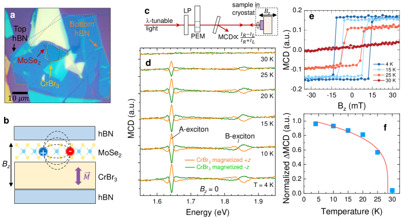
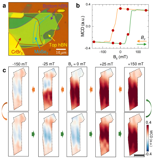
Figures 1a and 1b show an example of a MoSe2/CrBr3 heterostructure used in this study. All individual layers were mechanically exfoliated and stacked within an argon glovebox using standard dry transfer techniques (see Methods). The MoSe2 monolayer was placed on few-layer CrBr3 and sandwiched between hexagonal boron nitride (hBN) slabs to maintain high optical quality. CrBr3 is a 2D van der Waals magnet exhibiting out-of-plane ferromagnetic order below its Curie temperature Chen:Science:2019 ; Kim:PNAS:2019 ; Soriano:2020 ; Mak:2019 . The structures were assembled on Si substrates, mounted on a confocal microscope probe, and loaded into the variable-temperature helium insert of a magneto-optical cryostat. Magnetic fields could be applied normal to the sample plane in the Faraday geometry. MCD spectroscopy (depicted in Fig. 1c, and described in Methods) was used to characterize the overall splitting between and valleys in the MoSe2 monolayer, due to MPIs with the CrBr3 layer. To separately resolve the energy shifts induced at the and valleys of the MoSe2, the spectra of right- and left-circularly polarized reflected light were individually measured.
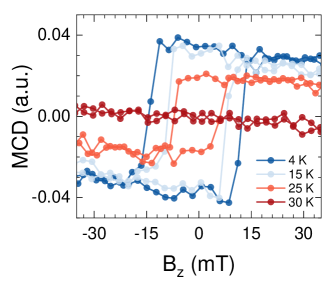
The presence of strong MPIs in these structures is revealed by the temperature-dependent MCD spectra shown in Fig. 1d. MCD, which detects the intensity difference between right- and left-circularly polarized light (in reflection or transmission), is inherently sensitive to phenomena that break time-reversal symmetry, such as magnetization. Crucially, all spectra in Fig. 1d were acquired at , after magnetizing the ferromagnetic CrBr3 along the or direction. Below the Curie temperature ( K), pronounced MCD signals remain at =0, at both of the fundamental A- and B-exciton resonances of the MoSe2 monolayer, indicating the presence of MPIs. Flipping the CrBr3 magnetization from to inverts the MCD signals (as expected), and the zero-field MCD signals disappear above . The particular lineshapes of the MCD resonances follow the derivatives of the A- and B-exciton resonances as measured in reflection (shown below in Fig. 3).
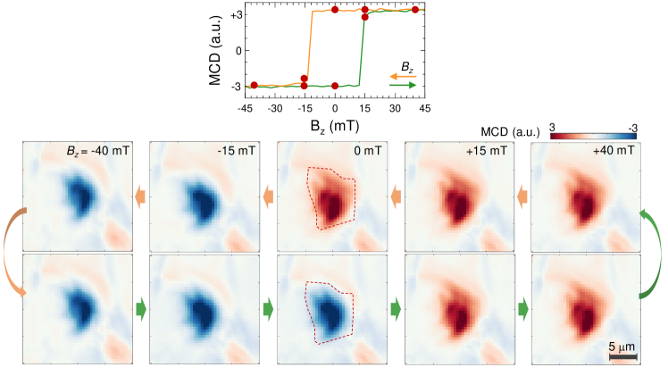
Figure 1e shows hysteresis loops of the MCD signal, acquired at the peak of the A-exciton resonance, when is varied between 40 mT, further confirming MPIs in these heterostructures. These data were taken using a wavelength-filtered xenon lamp, and the focused spot was approximately the same size as the sample itself (m). As such, the square hysteresis loops observed at low temperatures indicates that the entire CrBr3 flake behaves as a single magnetic domain that switches uniformly, and is devoid of multi-domain switching phenomena. The hysteresis loops collapse with increasing temperature and disappear above , in line with expectations. The MCD signal versus temperature, shown in Fig. 1f, is characteristic of the magnetization of ferromagnetic materials, and can be fit to the functional form , using =28 K and (red line), consistent with expectations of a Heisenberg spin system Fisher:critical:1974 ; Gilbertini:2019 . A set of MCD hysteresis loops acquired using probe light tuned to the B-exciton resonance shows essentially similar behavior, as expected (see Extended Data Fig. 1).
Spatially-resolved images of the MCD over the entire MoSe2/CrBr3 heterostructure (see Fig. 2) confirm that MPIs are approximately uniform over the entire structure, and that the CrBr3 layer behaves effectively as a single-domain magnet. For imaging, the probe light was derived from a continuous-wave Ti:S laser, and 1 m spatial resolution is achieved. MCD images at various applied around the hysteresis loop show a single domain structure, even near the coercive fields ( mT). MCD images of other vdW heterostructures having thicker CrBr3 showed multi-domain magnetic structure near the switching fields, as shown in Extended Data Fig. 2.
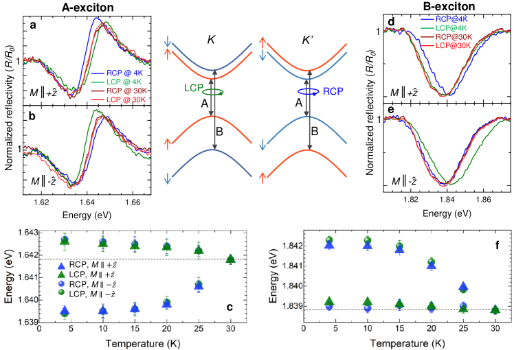
Having established the presence of strong MPIs in these hybrid structures, we now turn to the main result: In stark contrast to the influence of real magnetic fields, which shift time-reversed pairs of bands in the and valleys of MoSe2 equally and in opposite directions, we find that MPIs in these heterostructures are strongly asymmetric. That is, proximity-induced shifts of the exciton resonances have markedly different magnitudes in the and valleys. To separately analyze these shifts, we use circular-polarization-resolved, and therefore valley-resolved, optical reflection spectroscopy. (Note that MCD is less sensitive to such asymmetry, since it detects the difference between right- and left-circular polarization, and not the shift in each valley separately).
Figure 3a demonstrates this asymmetry. The blue and green traces show the 4 K reflection resonance of the A-exciton in the MoSe2 monolayer, for RCP and LCP light ( and valleys) respectively, when the CrBr3 is magnetized along the direction. To serve as a common reference and control experiment, the red and orange traces were acquired at 30 K (above ), where the CrBr3 is unmagnetized (and indeed, the red and orange spectra are identical to within experimental noise). Clearly, the magnitude of the energy shift at low temperature is noticeably larger in (blue trace) than in (green trace). This behavior contrasts with the valley Zeeman shifts arising from real applied magnetic fields, which shift the bands equally and in opposite directions Stier:2016 . Importantly, Fig. 3b shows that the LCP/RCP () asymmetry inverts when the CrBr3 is magnetized along the opposite direction (), confirming that the asymmetry is due to MPI interactions.
The individual energy shifts in the and valleys can be determined from fits of the reflection resonances to a complex-Lorentzian lineshape (see Methods), and tracked with good precision. The evolution of the asymmetric energy splitting as a function of temperature is shown in Fig. 3c. The asymmetry exceeds a factor of two, with an energy redshift of 2 meV in the valley that is accompanied by an opposite blueshift of only 1 meV in the valley (for the case of CrBr3 magnetization). The total energy splitting of 3 meV that is observed at low temperatures is commensurate with the (symmetric) valley splitting expected from a magnetic field of approximately 13 T, assuming a neutral A-exciton g-factor , in very good correspondence with prior work by Ciorciaro et al. Ciorciaro:PRL:2020 . We emphasize that the asymmetric shifts are not an artifact of any temperature-dependent band-gap shift arising from the 30 K ‘control’ spectra; redshifts of the bandgap between 4 K and 30 K are negligible, and furthermore if present would only make the observed asymmetry even more pronounced.
Interestingly, a rather different asymmetry is observed at the B-exciton of MoSe2, as shown in Fig. 3d. Here, MPIs induce a marked energy shift in the valley (when the CrBr3 is magnetized along ), but almost no discernible shift in the valley. Taken together, we therefore conclude that characterizing the valley splitting by a simple effective magnetic field is of limited utility, as it does not capture the marked asymmetry that clearly arises from MPIs. Figure 3e confirms that the asymmetry at the B-exciton inverts when the CrBr3 magnetization is flipped, and Fig. 3f shows the evolution of the MPI-induced energy shifts of the B-exciton as a function of temperature.
Comparing the energy shifts of the A- and B-excitons in Figs. 3c and 3f reveals another unexpected aspect of asymmetric MPIs: For a given CrBr3 magnetization, the dominant energy shifts for both A- and B-exciton transitions are not only of different sign, but are observed in the same valley. Considering the spin-dependent level structure of the conduction and valence bands in MoSe2 monolayers (see band diagram in Fig. 3), it might be anticipated that a spin-specific proximity interaction affecting (for example) only the spin-up bands, should cause shifts in the valley of the A-exciton, and in the valley of the B-exciton. These data demonstrate that the coupling between the electronic band structures of the two constituent materials is more complex.
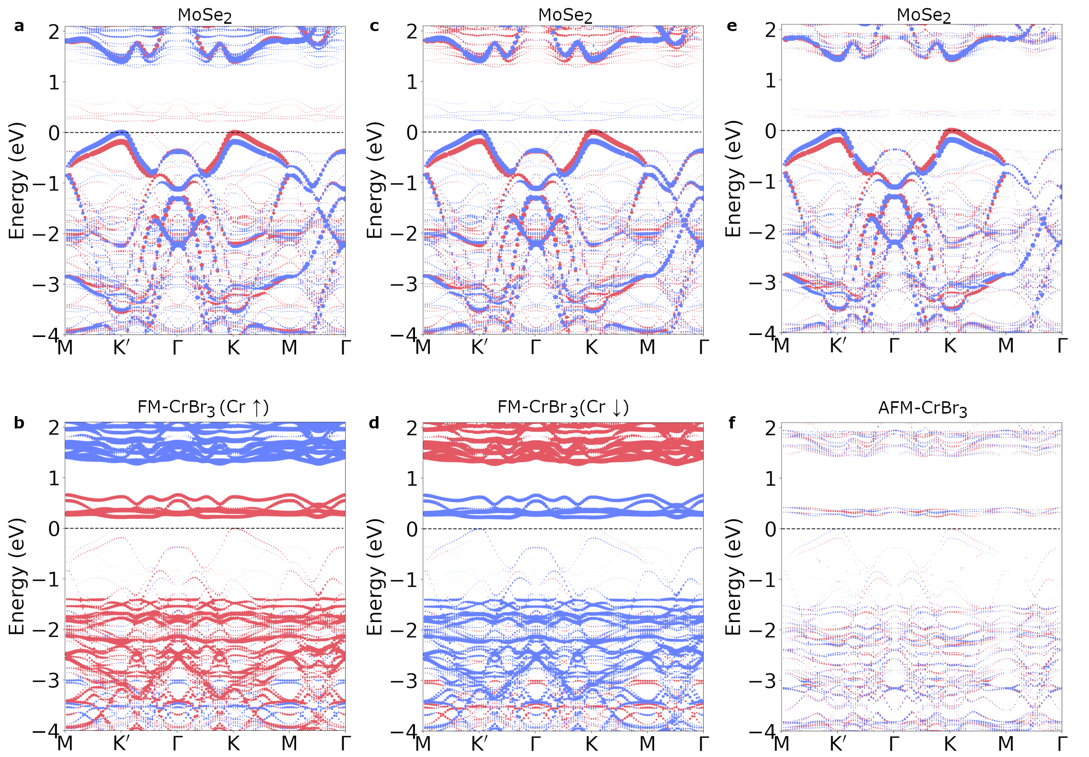
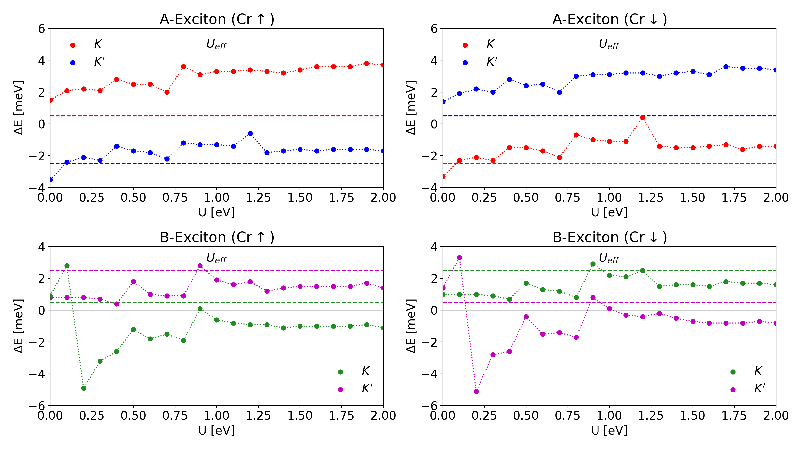
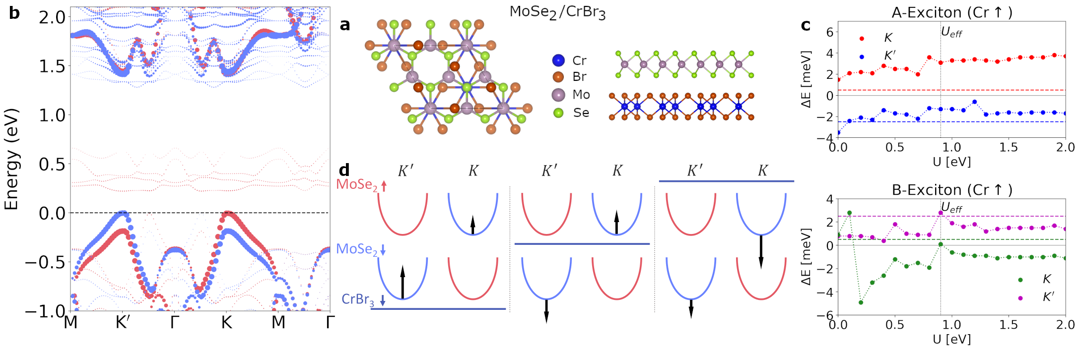
To provide insight into the asymmetric valley shifts driven by MPIs, we examined the electronic band structure of monolayer MoSe2 stacked on a single layer of CrBr3 (Fig. 4a) within the framework of density functional theory (DFT; see Methods). To most directly compare the MPI-induced energy shifts with experimental data (which includes control measurements in the non-magnetic phase of CrBr3), we considered two cases: (i) CrBr3 with out-of-plane ferromagnetic order, to capture the low-temperature phase, and (ii) CrBr3 with in-plane antiferromagnetic spin configuration, to simulate the high-temperature non-magnetic state and serve as a reference. We note that since the band energies are sensitive to the overall electronic environment and band alignment between the CrBr3 and MoSe2 layers (see for example Fig. 4b, or Extended Data Fig. 3), one cannot simply compare the band shifts with and without the CrBr3 layer, due to intrinsic interlayer coupling even in the non-magnetic phase.
Figure 4c shows the calculated shifts of the optical transition energies in the and valleys due to MPIs as function of band alignment between MoSe2 and CrBr3 layers (as controlled by the Hubbard ; see Methods), with the experimental values overlaid. A significant valley asymmetry is clearly revealed at both of the fundamental A and B optical transitions, in line with our valley-resolved reflection spectra. Specifically, a value of 0.9 eV simultaneously yields the experimental band gap of CrBr3 and the measured shifts of the optical transition energies. Here, our DFT results indicate asymmetric shifts with the same sign structure and valley dependence for both CrBr3 magnetization directions. In addition, the magnitudes of the calculated shifts are in reasonable and qualitative accord with experiment. Further refinements of the DFT values, beyond the scope of this work, may be obtained by employing GW quasiparticle corrections and calculating the full exciton spectrum within the Bethe-Salpeter equation framework. However, we stress that these calculations even at the DFT level already capture the essential trends and marked asymmetries shown in the experimental data.
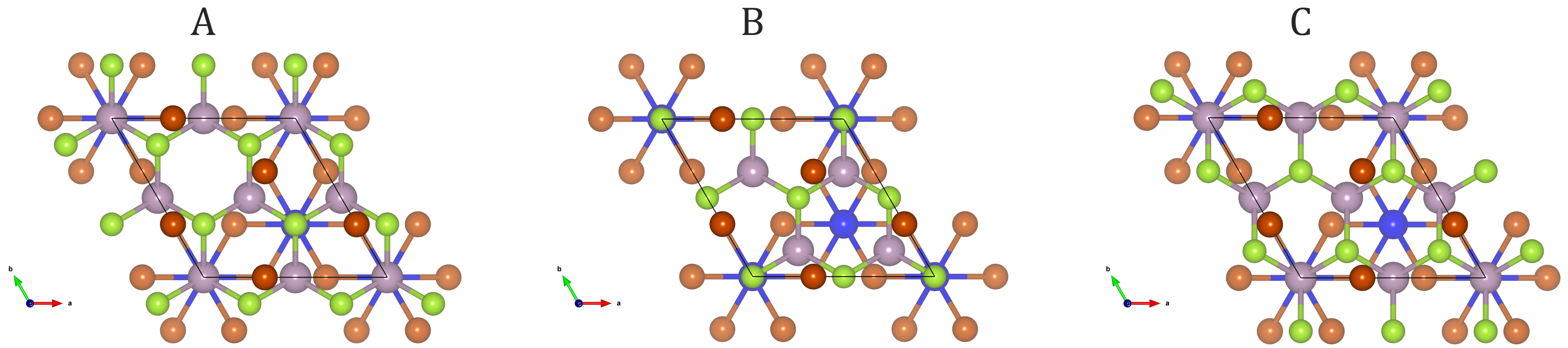
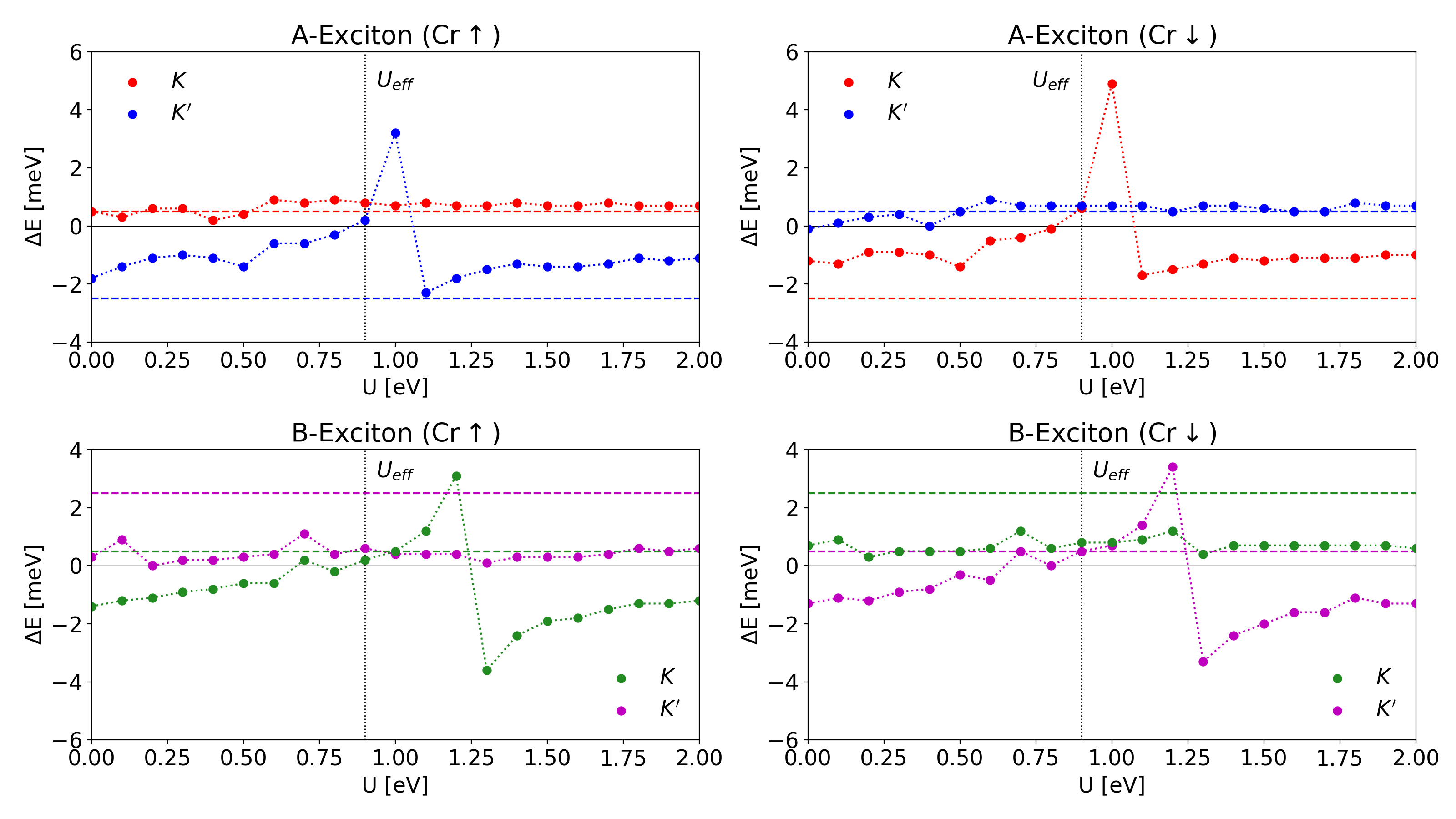
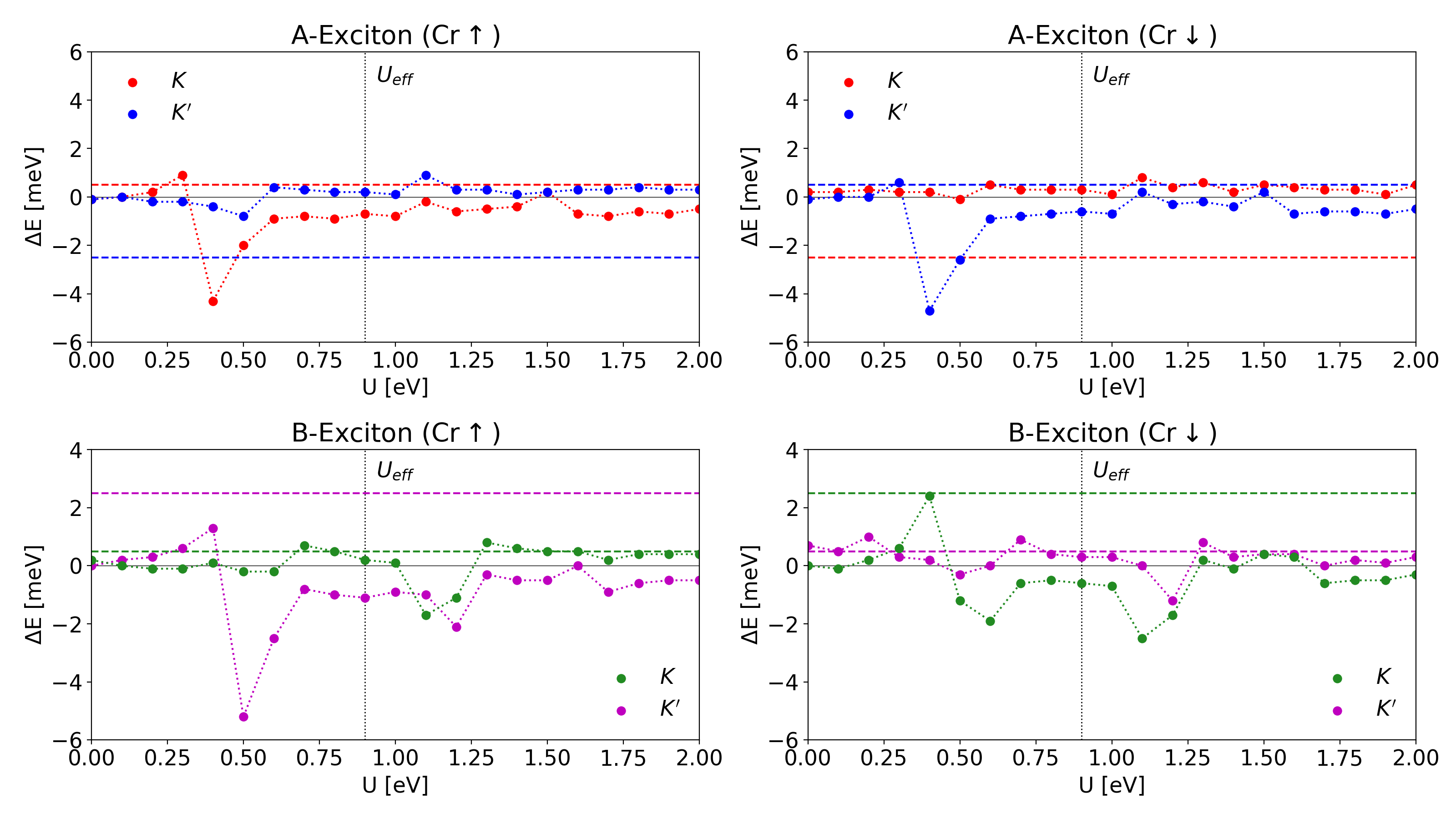
The asymmetric valley splittings due to MPIs can be understood as follows. Due to the band alignment between the CrBr3 and MoSe2 layers, the conduction states of both layers directly overlap and hybridize, as indicated by the weaker band features in the MoSe2 projected dispersions shown in Fig. 4b. Extended Data Fig. 3 explicitly shows the electronic bands projections for both CrBr3 and MoSe2 layers revealing the significant mixing between the electronic states of the layers. This hybridization drives resonant avoided crossing phenomena between same-spin bands, thereby producing strong band shifts, with magnitude and sign sensitively dependent on the detailed alignment of the constituent levels. Figure 4d shows a simplified illustration that highlights the essential physics: For various band alignments, like-spin MoSe2 conduction bands shift to avoid the upper (spin-polarized) bands of ferromagnetic CrBr3, yielding valley-dependent shifts of the optical transitions that differ qualitatively from a picture of simple Zeeman splitting. Due to the avoided-crossing behavior, the calculated band shifts have magnitude and sign that depend sensitively on the relative energies of the upper CrBr3 bands and the MoSe2 conduction bands, which marks a distinct departure from the effective magnetic field characterization typically employed to quantify MPIs. This behavior is directly seen in the calculated shifts (Fig. 4c) as peaks and troughs in the data, marking the energies at which the CrBr3 states cross the MoSe2 bands. (Note that the MoSe2 valence bands at and display an approximately symmetric valley splitting, as expected since they do not closely overlap with any states of the CrBr3 layer). Extended Data Figs. 4-7 demonstrate how, within our DFT approach, the calculated energy shifts and the degree of asymmetry evolve for different stacking arrangements of the constituent CrBr3 and MoSe2 layers, for various band alignments. These results also suggest that the band alignment and inter-layer coupling of a given magnetic heterostructure may be quantified by the experimentally-measured sign and magnitude of asymmetric valley shifts. The extent to which twist angle between the MoSe2 monolayer and the CrBr3 affects the valley shifts in such hybrid structures has not been explored here, and remains an open question.
By revealing the marked spin/valley asymmetries that can arise from MPIs in hybrid vdW structures, this work suggests routes toward selective control over specific spin and/or valley states in monolayer TMD semiconductors via rational design of the component materials, and also their stacking arrangement. Together with the additional tunability of MPIs that can arise from electrostatic gating (as demonstrated in graphene-based hybrid vdW heterostructures Kawakami:2018 ), and recent predictions of gate-tunable band topology in monolayer semiconductors Tong:2020 , these results complement the set of available tools with which future spin- and valley-dependent (opto)electronic devices may be engineered. Moreover, our experimental data and DFT calculations strongly indicate that asymmetric magnetic proximity interactions are likely a universal aspect of hybrid vdW heterostructures, manifesting especially in material combinations where electronic bands overlap closely in energy.
METHODS
Sample preparation. Monolayer MoSe2 (2D Semiconductors) and hBN flakes were mechanically exfoliated from bulk crystals onto Si substrates under ambient conditions and moved into an argon glovebox. O2 and H2O concentrations in the glovebox were maintained below 0.1 ppm. Few-layer flakes of CrBr3 (HQ graphene) were exfoliated onto Si substrates inside the glovebox. MoSe2/CrBr3 heterostructures were assembled by standard dry transfer techniques Kim:transfer:2016 using polycarbonate stamps, and were sandwiched between hBN slabs. Then the samples were moved out of the glovebox and washed in chloroform to remove polymer residues. The thickness of the CrBr3 (typically 5 layers) was identified by atomic force microscopy after the polymer residue was removed. The samples were mounted on a confocal microscope probe and loaded into the variable-temperature helium-flow insert of a 7 T superconducting magnet with direct optical access.
MCD spectroscopy and imaging. Broadband MCD spectroscopy was performed in a reflection geometry using wavelength-tunable narrowband light derived from a xenon white light source filtered through a 300 mm spectrometer. The probe light was intensity-modulated by mechanical chopper, and then modulated between right- and left-circular polarizations by a linear polarizer and photoelastic modulator (PEM). The light was focused to a small spot (approximately m) on the sample by an aspheric lens that was controlled by a piezo nanopositioner (attocube). The back-reflected light from the sample was collected by the same lens and directed by a beamsplitter to an avalanche photodiode detector (as depicted in Fig. 1c). The signal was demodulated by two lock-in amplifiers, referenced to the chopper and PEM frequencies (137 Hz and 50 kHz, respectively). MCD is given by the normalized difference between the right- and left-circularly polarized reflected intensities, . For the MCD imaging experiments shown in Fig. 2, the probe light was derived instead from a wavelength-tunable continuous-wave Ti:sapphire ring laser, so that much better spatial resolution could be achieved (1 m focused spot size). The incident probe laser beam was coupled to a 2D galvo mirror scanner for raster scanning and spatial imaging.
Polarization- (valley-) resolved reflection spectroscopy. The polarization-resolved reflection measurements were performed using the same confocal microscope described above. Here, broadband white light from a xenon lamp was coupled into a single-mode fiber, then collimated by an achromatic lens, and then circularly polarized using a linear polarizer and quarter-wave plate. The white light was then focused to a 1 m spot with an aspheric lens. The reflected light from the sample was collected by a multi-mode fiber and detected by a cooled charge-coupled device (CCD) detector. As is typical for reflection spectroscopy of vdW heterostructures, the A- and B-exciton resonances exhibit a complex-Lorentzian lineshape xfermatrix (i.e., having both dispersive and absorptive components to the lineshape). Once a fit was established at a given temperature, the temperature-dependent shift of the transition energy (see Fig. 3) was accurately tracked by fixing all parameters except for the resonance energy. Alternatively, letting all fit parameters float yielded essentially identical results, because the lineshape remains unchanged.
Density functional theory calculations. Density functional theory (DFT) based first-principles electronic structure calculations were carried out by using the pseudopotential projector-augmented wave method Kresse1999 implemented in the Vienna ab initio simulation package (VASP) Kresse1996 ; Kresse1993 . We used an energy cutoff of eV for the plane-wave basis set. Exchange-correlation effects were treated using the Perdew-Burke-Ernzerhof (PBE) GGA density functional Perdew1996 . A -centered k-point mesh was used to sample the Brillouin zone. Spin-orbit coupling effects were included self-consistently. An effective Hubbard was added to the Cr-3 orbitals Dudarev to control the band alignment and correct the band gap of the magnetic layer. A of 0.9 eV was found to yield the experimental band gap of CrBr3 and the asymmetric optical transitions simultaneously. The heterobilayer was constructed from a unit cell of CrBr3 and a super cell of MoSe2. To not alter the electronic structure of the MoSe2 layer, we strained CrBr3 to make both layers commensurate Kormanyos2015 . Three distinct stacking configurations were considered, as shown in the Extended Data. To ensure negligible interaction between the periodic images of the bilayer film, a large enough vacuum of 19 Å in the -direction was used. Finally, all atomic sites in the unit cell were relaxed simultaneously using a conjugate gradient algorithm to minimize energy with an atomic force tolerance of eV/Å and a total energy tolerance of eV. The unfolded band structure was obtained using the PyProcar package pyprocar .
Acknowledgements We gratefully acknowledge Igor Žutić and Bernhard Urbaszek for helpful discussions. Experimental studies at the NHMFL were supported by the Los Alamos LDRD program. The NHMFL is supported by National Science Foundation (NSF) DMR-1644779, the State of Florida, and the U.S. Department of Energy (DOE). Computational studies were supported in part by the Center for Integrated Nanotechnologies, a DOE BES user facility, in partnership with the LANL Institutional Computing Program for computational resources.
References
- (1) Žutić, I., Matos-Abiague, A., Scharf, B., Dery, H. & Belashchenko, K. Proximitized Materials, Materials Today, 22, 85 (2019).
- (2) Gibertini, M., Koperski, M., Morpurgo, A. F. & Novoselov, K. S. Magnetic 2D materials and heterostructures, Nat. Nanotechnol. 14, 408–419 (2019).
- (3) Mak, K. F., Shan, J. & Ralph, D. Probing and controlling magnetic states in 2D layered magnetic materials, Nat. Rev. Phys. 1, 646-661 (2019).
- (4) Zhao, C., Norden, T., Zhang, P., Zhao, P., Cheng, Y., Sun, F., Parry, J. P., Taheri, P., Wang, J., Yang, Y., Scrace, T., Kang, K., Yang, S., Miao, G.-X., Sabirianov, R., Kioseoglou, G., Huang, W., Petrou, A. & Zeng, H. Enhanced valley splitting in monolayer WSe2 due to magnetic exchange field, Nat. Nanotechnol. 12, 757-762 (2017).
- (5) Zhong, D., Seyler Kyle, L., Linpeng, X., Cheng, R., Sivadas, N., Huang, B., Schmidgall, E., Taniguchi, T., Watanabe, K., McGuire Michael, A., Yao, W., Xiao, D., Fu K.-M. C. & Xu, X. Van der Waals engineering of ferromagnetic semiconductor heterostructures for spin and valleytronics, Sci. Adv. 3, e1603113 (2017).
- (6) Norden, T., Zhao, C., Zhang, P., Sabirianov, R., Petrou, A. & Zeng, H. Giant valley splitting in monolayer WS2 by magnetic proximity effect, Nat. Commun. 10, 4163 (2019).
- (7) Ciorciaro, L., Kroner, M., Watanabe, K., Taniguchi, T. & Imamoglu, A. Observation of Magnetic Proximity Effect Using Resonant Optical Spectroscopy of an Electrically Tunable MoSe2/CrBr3 Heterostructure, Phys. Rev. Lett. 124, 197401 (2020).
- (8) Zhong, D., Seyler, K. L., Linpeng, X., Wilson, N. P., Taniguchi, T., Watanabe, K., McGuire, M. A., Fu, K.-M. C., Xiao, D., Yao, W. & Xu, X. Layer-resolved magnetic proximity effect in van der Waals heterostructures, Nat. Nanotechnol. 15, 187-191 (2020).
- (9) Xiao, D., Liu, G.-B., Feng, W., Xu, X. & Yao, W. Coupled Spin and Valley Physics in Monolayers of MoS2 and Other Group-VI Dichalcogenides, Phys. Rev. Lett. 108, 196802 (2012).
- (10) Xu, X., Yao, W., Xiao, D. & Heinz, T. F. Spin and pseudospins in layered transition metal dichalcogenides. Nat. Phys. 10, 343-350 (2014).
- (11) Lazić, P., Belashchenko, K. D. & Žutić, I. Effective gating and tunable magnetic proximity effects in two-dimensional heterostructures, Phys. Rev. B 93, 241401(R) (2016)
- (12) Xu, J., Singh, S., Katoch, J., Wu, G., Zhu, T., Žutić, I. & Kawakami, R. Spin inversion in graphene spin valves by gate-tunable magnetic proximity effect at one-dimensional contacts, Nat. Commun. 9, 2869 (2018).
- (13) Mak, K. F. & Shan, J. Photonics and optoelectronics of 2D semiconductor transition metal dichalcogenides, Nat. Photon. 10, 216-226 (2016).
- (14) Wang, G., Chernikov, A., Glazov, M. M., Heinz, T. F., Marie, X., Amand, T. & Urbaszek, B. Excitons in atomically thin transition metal dichalcogenides, Rev. Mod. Phys. , 90, 021001 (2018).
- (15) Wang, Q. H., Kalantar-Zadeh, K., Kis, A., Coleman, J. N. & Strano, M. S. Electronics and optoelectronics of two-dimensional transition metal dichalcogenides, Nature Nanotechnology 7, 699-712 (2012).
- (16) Schaibley, J. R., Yu, H., Clark, G., Rivera, P., Ross, J. S., Seyler, K. L., Yao, W. & Xu, X. Valleytronics in 2D materials, Nat. Rev. Mater. 1, 16055 (2016).
- (17) Qi, J., Li, X., Niu, Q. & Feng, J. Giant and tunable valley degeneracy splitting in MoTe2, Phys. Rev. B 92, 121403(R) (2015).
- (18) Zhang, Q., Yang, S. A., Mi, W., Cheng, Y. & Schwingenschlögl, U. Large Spin-Valley Polarization in Monolayer MoTe2 on Top of EuO(111), Adv. Mater. 28, 959 (2016)
- (19) Scharf, B., Xu, G., Matos-Abiague, A. & Žutić, I. Magnetic Proximity Effects in Transition-Metal Dichalcogenides: Converting Excitons, Phys. Rev. Lett. 119, 127403 (2017).
- (20) Zollner, K., Faria Junior, P. E. & Fabian, J. Proximity effects in MoSe2 and WSe2 heterostructures with CrI3: Twist angle, layer, and gate dependence. Phys. Rev. B 100, 085128 (2019).
- (21) Zhang, Z., Ni, X., Huang, H., Hu, L. & Liu, F. Valley splitting in the van der Waals heterostructure WSe2/CrI3: The role of atom superposition. Phys. Rev. B 99, 115441 (2019).
- (22) Xie J., Jia, L., Shi, H., Yang, D. & Si, M., Electric field mediated large valley splitting in the van der Waals heterostructure WSe2/CrI3, Jpn. J. Appl. Phys. 58, 010906 (2019)
- (23) Lyons, T. P., Gillard, D., Molina-Sánchez, A., Misra, A., Withers, F., Keatley, P. S., Kozikov, A., Taniguchi, T., Watanabe, K., Novoselov, K. S., Fernández-Rossier, J. & Tartakovskii, A. I. Interplay between spin proximity effect and charge-dependent exciton dynamics in MoSe2/CrBr3 van der Waals heterostructures, Nat. Commun. 11, 6021 (2020).
- (24) Chen, W., Sun, Z., Wang, Z., Gu, L., Xu, X., Wu, S. & Gao, C. Direct observation of van der Waals stacking–dependent interlayer magnetism, Science 366, 983-987 (2019).
- (25) Kim, H. H., Yang, B., Li, S., Jiang, S., Jin, C., Tao, Z., Nichols, G., Sfigakis, F., Zhong, S., Li, C., Tian, S., Cory, D. G., Miao, G.-X., Shan, J., Mak, K. F., Lei, H., Sun, K., Zhao, L. & Tsen, A. W. Evolution of interlayer and intralayer magnetism in three atomically thin chromium trihalides, Proc. Natl. Acad. Sci. U.S.A. 116, 11131-11136 (2019).
- (26) Soriano, D., Katsnelson, M. I. & Fernandez-Rossier, J. Magnetic Two-Dimensional Chromium Trihalides: A Theoretical Perspective, Nano Lett. 20, 6225-6234 (2020).
- (27) Fisher, M. E. The renormalization group in the theory of critical behavior, Rev. Mod. Phys. 46, 597-616 (1974).
- (28) Stier, A. V., McCreary, K. M., Jonker, B. T., Kono, J. & Crooker, S. A. Exciton diamagnetic shifts and valley Zeeman effects in monolayer WS2 and MoS2 to 65 Tesla. Nat. Commun. 7, 10643 (2016).
- (29) Xu, G., Zhou, T., Scharf, B. & Žutić, I., Optically Probing Tunable Band Topology in Atomic Monolayers, Phys. Rev. Lett. 125, 157402 (2020).
- (30) Kim, K., Yankowitz, M., Fallahazad, B., Kang, S., Movva, H. C., Huang, S., Larentis, S., Corbet, C. M., Taniguchi, T., Watanabe, K., Banerjee, S. K., LeRoy, B. J. & Tutuc, E. van der Waals Heterostructures with High Accuracy Rotational Alignment, Nano Lett. 16, 1989-1995 (2016).
- (31) Robert, C. et al., Optical spectroscopy of excited exciton states in MoS2 monolayers in van derWaals heterostructures, Phys. Rev. Mater. 2, 011001(R) (2018).
- (32) Kresse, G. & Joubert, D. From ultrasoft pseudopotentials to the projector augmented-wave method, Phys. Rev. B 59, 1758 (1999).
- (33) Kresse, G. & Furthmüller, J. Efficient iterative schemes for ab initio total-energy calculations using a plane-wave basis set, Phys. Rev. B 54, 11169 (1996).
- (34) Kresse, G. & Hafner, J.J. Ab initio molecular dynamics for open-shell transition metals, Phys. Rev. B 48, 13115 (1993).
- (35) Perdew, J. P., Burke, K. & Ernzerhof, M. Generalized gradient approximation made simple, Phys. Rev. Lett. 77, 3865 (1996).
- (36) Dudarev, S. L., Botton, G. A., Savrasov, S. Y., Humphreys, C. J. & Sutton, A. P. Electron-energy-loss spectra and the structural stability of nickel oxide: An LSDA+U study Phys. Rev. B 57, 1505 (1998).
- (37) Kormányos, A., Burkard, G., Gmitra, M., Fabian, J., Zólyomi, V., Drummond, N. D. & Fal’ko, V. k· p theory for two-dimensional transition metal dichalcogenide semiconductors, 2D Mater. 2, 022001 (2015).
- (38) Herath, U. et al. Computer Phys. Comm. 251, 107080 (2020).