Heating-compensated constant-temperature tunneling measurements on stacks of Bi2Sr2CaCu2O8+x intrinsic junctions
Abstract
In highly anisotropic layered cuprates such as Bi2Sr2CaCu2O8+x tunneling measurements on a stack of intrinsic junctions in a high-bias range are often susceptible to self-heating. In this study we monitored the temperature variation of a stack (“sample stack”) of intrinsic junctions by measuring the resistance change of a nearby stack (“thermometer stack”) of intrinsic junctions, which was strongly thermal-coupled to the sample stack through a common Au electrode. We then adopted a proportional-integral-derivative scheme incorporated with a substrate-holder heater to compensate the temperature variation. This in-situ temperature monitoring and controlling technique allows one to get rid of spurious tunneling effects arising from the self-heating in a high bias range.
pacs:
74.72.Hs 74.50.+r 74.25.Fy 44.10.+iSince the discovery of the intrinsic Josephson effect in highly anisotropic layered Bi2Sr2CaCu2O8+x (Bi-2212) high- single crystals Kleiner , tunneling characteristics along the axis have been extensively investigated using the mesa structure prepared on the crystal surface to probe the interlayer coupling characteristics as well as the superconducting properties of the Cu-O layers themselves mesa . Superconducting properties of Bi-2212 crystals have also been examined using tunneling in artificial surface junctions or the scanning tunneling spectroscopy Renner . In this case, however, tunneling properties are susceptible to any surface degradation. The advantage of tunneling measurements using intrinsic junctions, in comparison, is that one can eliminate the surface-dependent effect.
The poor thermal conductivity of the Bi-2212 intrinsic junctions, however, is known to cause serious local self-heating in tunneling measurements, when a high-density bias current is used Krasnov ; heat . The resulting temperature variation often causes a serious spurious effect in the tunneling signal. Much effort has been made to avoid self-heating by reducing the lateral size and the thickness of the mesa, the contact resistance, and by employing the pulsed bias method mesa ; pulse . Taking these precautions, one can reduce the back-bending effect (negative dynamics resistance) in the current-voltage () curve, which is mainly caused by self-heating in a high-bias range. In-situ temperature measurements in the above configurations, however, show that, even in the absence of the back bending, the self-heating still persists and can significantly distort tunneling measurements. ratio ; Yurgens
In this letter we present a scheme of making tunneling measurements in a stack of intrinsic junctions at a constant temperature in any finite bias currents. Our samples consisted of two separate stacks of intrinsic junctions which were closely coupled laterally by a common Au electrode [inset of Fig. 1(b)]. We monitored the temperature of the stack of interest [“sample stack (SmS)”] including self-heating, which was then compensated using the proportional-integral-derivative (PID) temperature control method with another stack of intrinsic junctions [“thermometer stack (ThS)”] as a thermometer and using a substrate-holder heater.
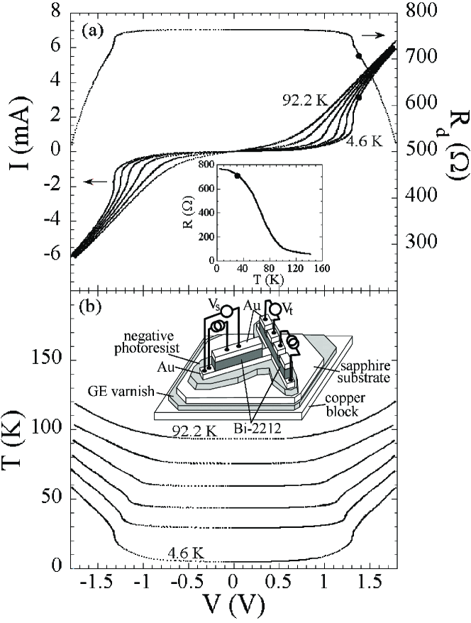
Bi-2212 single crystals were grown by the solid-state-reaction method Kim . In this study, two samples [SH1 and SH2] were fabricated, where the double-side-cleaving of Bi-2212 crystals, micropatterning, and ion-beam etching were employed Bae . Resistive transition of the two samples exhibited that SH1 was slightly underdoped (=85.8 K, =0.21) and SH2 was almost optimally doped (=90.3 K, =0.23) Suzuki . The inset of Fig. 1(b) shows the sample geometry and the measurement configuration. The left and right stacks are the SmS and the ThS, respectively. The lateral dimensions of the SmS in SH1 and SH2 were 15.31.6 and 16.21.6 m2, respectively. The ThS was placed laterally 1.4 and 1.6 m apart from the SmS for SH1 and SH2, respectively, and was thermally coupled by a 100-nm-thick common Au electrode [inset of Fig. 1(b)]. Contrary to the case of a mesa structure, without the poorly thermal-conductive Bi-2212 basal part in this geometry, the heat generated in the SmS diffuses effectively through the highly thermal-conductive (=100 W/mK) bottom Au electrode, thus putting both the SmS and ThS in the thermal equilibrium presumably at an almost equal temperature. The tunneling characteristics of the SmS and the ThS were measured in two- and three-terminal configurations, respectively, with the Au common ground electrode.
In our SmS without the basal part the temperature is almost uniformly distributed along the axis. For instance, the SmS of SH1 (containing =25 intrinsic junctions) was 37.5 nm thick. According to the thermal-conduction relation, =, with the top junction in the normal state in a high bias current density , the temperature difference between top and bottom of the stack is predicted to be only 0.8 K. In this estimate, the -axis critical current density of =0.6 kAcm-2, the voltage over each junction of =30 mV, and the -axis thermal conductivity of =0.009 W/mK at =4.2 K, were used Krasnov . If all the junctions in the SmS are driven to the normal state the whole SmS acts as a heating element and the temperature will become more uniform.
The temperature increase in the ThS due to self-heating of the SmS reduces the gap energy and the quasiparticle tunneling resistance of the ThS. The inset of Fig. 1(a) shows the vs curve of the ThS of SH1 in the bias current of 0.1 mA, which is slightly above its tunneling critical current at 4.6 K. The temperature of the ThS was monitored by measuring the variation of the quasiparticle tunneling resistance in the bias of 0.1 mA, while the bias current of the SmS was swept continuously. To illustrate the temperature monitoring scheme, one first notices in Fig. 1(a) that the bias current of 2.8 mA, for instance, corresponds to the voltage value of 1.3 V in the SmS as denoted by a dot on the curve at 4.6 K. As illustrated with the right vertical scale, under these circumstances, the quasipariticle resistance of the ThS was reduced from 760 , corresponding to =4.6 K, to 720 because of the heat flow from the SmS. According to the vs curve in the inset of Fig. 1(a), the reduced resistance indicates that, due to self-heating, the temperature of both stacks increased from 4.6 K to 30 K.
Fig. 1(b) displays the variation of the actual temperature of the SmS, determined in the way described above along with the curves shown in Fig. 1(a), for different biases and the substrate-holder temperatures. In principle, the bias current of 0.1 mA in the ThS may also generate self-heating. The characteristics of the SmS with and without a bias current in the ThS, however, showed no noticeable difference between the two cases (data not shown). In our samples the averaged heating ratio (, the temperature increase per dissipated power) was 5 K/mW at 4.2 K, which was at least an order lower than the previously reported value of 50 K/mW in the mesa structure ratio ; Yurgens .
Although the elimination of the basal Bi-2212 part and the strong thermal coupling through the Au ground electrode reduced the heating ratio the self-heating was not completely eliminated. The main cause of the self-heating was the poor thermal conductivity of the gluing materials used. Negative photoresist was used to fix the Au-sandwiched Bi-2212 stack to the sapphire substrate, which in turn was attached to the copper substrate holder by GE varnish. The thermal conductivity of GE varnish, 0.08 W/mK (at =10 K), is much smaller than that of sapphire of 20 W/mK. The photoresist is expected to have even poorer thermal conductivity than GE varnish.
To illustrate the usefulness of our PID temperature control scheme we performed the tunneling spectroscopy using SH2 at fixed temperatures. The PID system consisted of a manganin heater coiled around the substrate holder, where the feedback current was determined by the relation Chan ,
| (1) |
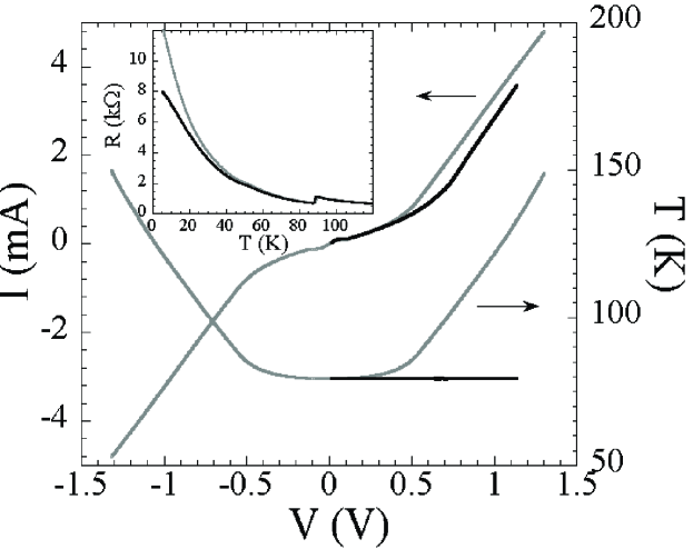
Here, is the difference between the set temperature and the actual temperature of the stacks. And is the proportional gain, the integration time constant, and the time rate constant. To monitor the temperature of the SmS of SH2, using the vs curves of the ThS, the ThS was biased by 0.28 mA, which was slightly above the tunneling critical current of SH2. As illustrated in the inset of Fig. 2, the higher bias current in SH2 than in SH1, caused serious self-heating. The gray and black solid lines in the inset are the vs curves of the SmS (= 0.5 A) in zero current and 0.28 mA in the ThS, respectively. Using these two vs curves we eliminated any additional error in reading temperatures due to the bias current of 0.28 mA in SH2.
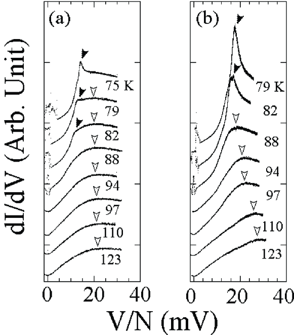
Fig. 2 shows the curves of SH2 without (the upper gray curve) and with (the upper black curve) adopting the PID scheme. The sweep speed of the bias in the SmS with the PID scheme was 50 Hz, much slower than 1 mHz without the PID scheme. The lower gray and black curves in Fig. 2 illustrate the temperature variation of the SmS as a function of the voltage in the cases without and with the PID scheme, respectively. Without the PID scheme, for the substrate-holder and bath temperatures at 79 K and 4.2 K, respectively, the temperature corresponding to the bias voltage of 1 V was 120 K. Using the PID scheme with the parameters =20, =10, and =1.2, however, the temperature of the SmS was kept fixed at 790.4 K for all the biases used. For higher biases further decrease of the substrate-holder temperature is required to keep the SmS temperature constant, which limits the varying ranges of the bias and the substrate-holder temperature. The window of the varying range of the two parameters shrinks for lower set temperatures of the SmS. For this reason, in this study, the tunneling measurements could be done for temperatures only above 40 K.
Fig. 3 shows the temperature dependence of the dynamical tunneling conductance (obtained by the lock-in technique) of SH2 near . Here, the bias voltage values were normalized by the number of junctions, =44. The open arrows in the figure indicate the maximum positions of the humps, which can be used to estimate the size of the pseudogap. On the other hand, the filled arrows indicate the superconducting gap edges. As reported previously mesa and in Fig. 3(a), without employing the PID scheme, the maximum positions of the humps are almost insensitive to temperature variation. As in Fig. 3(b), however, when the temperature of the stack was kept fixed by employing the the PID scheme for a set of conductance data, the maximum positions of the humps increase with increasing temperature above . In addition, without the PID scheme the superconducting gap and pseudogap have separate values near (93.5 K) of SH2, but they tend to merge into one with the PID scheme. The implication of these results should be reexamined.
In conclusion, we devised a PID scheme to keep the temperature of stacks of intrinsic junctions constant in a bias current by compensating the temperature increase of the stacks due to self-heating with lowering the substrate-holder temperature. We demonstrated, with an example of tunneling-spectroscopic measurements, that eliminating the self-heating is essential in obtaining intrinsic tunneling properties for any high biases in highly anisotropic layered cuprates such as Bi-2212.
The authors wish to acknowledge valuable discussion with V. M. Krasnov in Chalmers University of Technology as well as Y.-B. Kim and M.-S. Shin in POSTECH. This work was supported by the National Research Laboratory project administrated by KISTEP and also by the AOARD of the US Air Force by the Contract No. FA5209-04-P-0253.
References
- (1) R. Kleiner et al., Phys. Rev. Lett. 68, 2394 (1994).
- (2) M. Suzuki and T. watanabe, Phys. Rev. Lett. 82, 5361 (1999); V. M. Krasnov et al., Phys. Rev. Lett. 84, 5860 (2000).
- (3) Ch. Renner et al., Phys. Rev. Lett. 80, 149 (1998).
- (4) V. M. Krasnov et al., J. Appl. Phys 89, 5578 (2001).
- (5) J. C. Fenton and C. E. Gough, J. Appl. Phys 94, 4665 (2003); V. N. Zavaritsky, Phys. Rev. Lett. 92, 259701 (2004).
- (6) J. C. Fenton et al., Appl. Phys. Lett. 80, 2535 (2002); K. Anagawa et al., Appl. Phys. Lett. 83, 2381 (2003).
- (7) P. J. Thomas et al., Physica C 341-348, 1547 (2000); V. M. Krasnov et al., cond-mat/0410207 (2004).
- (8) A. Yurgens et al., Phys. Rev. Lett. 92, 259702 (2004).
- (9) N. Kim et al., Phys. Rev. B 59, 14639 (1999).
- (10) M.H. Bae et al., Appl. Phys. Lett. 83, 2187 (2003)
- (11) M. Suzuki and T. watanabe, Phys. Rev. Lett. 85, 4787 (2000).
- (12) C. K. Chan, Rev. Sci. Instrum. 59, 1001 (1988).