Admixtures to -wave gap symmetry in untwinned YBa2Cu3O7 superconducting films measured by angle-resolved electron tunneling
Abstract
We report on an ab-anisotropy of and in ramp-edge junctions between untwinned YBa2Cu3O7 and -wave Nb. For these junctions, the angle with the YBa2Cu3O7 crystal -axis is varied as a single parameter. The A()-dependence presents 2-fold symmetry. The minima in at suggest a real -wave subdominant component and negligible -wave or imaginary -wave admixtures. The ()-dependence is well-fitted by -, isotropic - and anisotropic -wave order parameter symmetry, consistent with .
pacs:
74.20.Rp, 74.50.+r, 74.72.Bk, 74.78.Bz, 85.25.-jPhase-sensitive experimentsWollmann:1993 ; Tsuei:1994 and tunnel spectroscopyWei:1998 have provided rich evidence for the sign change of the pair wave function in the crystal -plane of high- superconductors. Insight in the extent of subdominant admixtures to the -wave symmetry is less well established. They are of high importance for the basic understanding of high- superconductivity and the design of novel -wave based Josephson devices, but also for standard high- junctions. They determine for instance the exact position of the nodes, and the amount of -anisotropy.
In YBa2Cu3O7 strong anisotropy in the electronic structure has been reported, which can be interpreted as an effective mass anisotropy along the - and -axes: An elongated vortex shape by scanning tunneling spectroscopy Maggio:1995 suggests 50 anisotropy. Sixty percent anisotropy is found in the London penetration depth by far-infrared spectroscopy,Basov:1995 as well as using -axis YBa2Cu3O7/Pb Josephson junctions with a magnetic field oriented parallel to the - or -axis.Sun:1995 Other studies, neutron scattering on flux-line lattices Johnson:1999 and single crystal torque-measurements,Ishida:1996 indicate a smaller anisotropy of . Related, surface impedance Zhang:1994 and resistivity measurements Friedmann:1990 demonstrate an anisotropy of to and respectively.
Also, implications for the anisotropy of the superconducting gap have been discussed. Raman scattering Limonov:1998 evidences a real isotropic -wave admixture of 5; thermal conductivity measurements in a rotating magnetic field Aubin:1997 place a maximum of 10% based on the node positions. Angle-resolved photoemission spectroscopy (ARPES)Aet:2001 indicates larger -anisotropy of . The use of untwinned single-crystals is considered crucial in all these studies. However, clear consensus on subdominant order parameter symmetries is not reached, nor is detailed angle-resolved data in the -plane of thin films available, although first attempts on twinned films have been performed.van:1999 In view of this, we present here new results on the anisotropy, comparing untwinned and twinned YBa2Cu3O7.
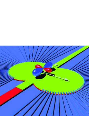
In untwinned YBa2Cu3O7 thin films, the usual ‘random’ exchange of the - and -axis is eliminated. This enables to study the electronic properties angle-resolved in the -plane. The experimental layout is summarized in Fig. 1. Basically, the YBa2Cu3O7 base-electrode is patterned into a nearly circular polygon, changing the orientation from side to side by 5 degrees. A Au barrier and Nb counter-electrode contact each side. In this way, the angle with respect to the -orientation is varied as a single parameter.
First, bilayers of 170 nm YBa2Cu3O7 and 100 nm SrTiO3 are grown by pulsed-laser deposition (PLD) on single-crystal SrTiO3 substrates. The YBa2Cu3O7 films are optimally doped, with 89 K. Ramps are ion-milled in the bilayers using a photo resist stencil. To assure equivalent ramp quality over , the sample stage is rotated around the substrate normal, while maintaining the angle of incidence of the Ar-ion beam constant at with the substrate plane. The resulting ramp-angle with the substrate plane is . On a microscopic scale the interfaces may present some faceting, albeit less than in e.g. grain boundaries. This faceting is not expected to affect the main conclusions of the presented studies. After removal of the photo-resist stencil and a short -incidence ion-mill for cleaning purposes, a 5 nm YBa2Cu3O7 interlayer Smilde:2002 is deposited to prepare an in-situ interface to a 30 nm Au barrier formed also by PLD. Then, a 160 nm thick Nb counter-electrode is dc-sputter deposited through a lift-off stencil. Special care is taken to obtain a clean Au/Nb interface by a 50 s rf-plasma etch just before Nb deposition. After lift-off, redundant Au and YBa2Cu3O7 interlayer material is removed by Ar-ion milling. The junctions are 4 m wide.
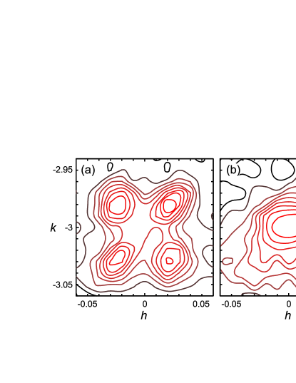
The twin behavior of -YBa2Cu3O7 films is influenced by the substrate vicinal angle and its in-plane orientation .Dekkers:2003 Here, is defined between the crystallographic and optical substrate-normal, and describes the in-plane orientation with respect to the SrTiO3 crystal axis. The degree of twinning can be controlled from completely untwinned to the presence of four -orientations, varying from to a small vicinal angle ( ), where . For , growth with the -axis along the step-ledges is induced, and only one crystal orientation is present. On the contrary, 4 twin orientations are present for small vicinal angle substrates. The twin orientations have pair-wise their in-plane diagonal of the YBa2Cu3O7 crystal aligned with each substrate diagonal, so that - and -axes and vice versa are arranged nearly in parallel.Dekkers:2003 After completion of the device, the YBa2Cu3O7 base-electrode is examined with X-ray diffraction (XRD). An average of the and unit cell dimensions is found for twinned films (see Table 1). For untwinned films, the individual and unit cell parameters can be distinguished and are close to single-crystal values. Detailed -scans of the reflections show 4 different orientations for YBa2Cu3O7 films grown on small vicinal angle substrates (Fig. 2a), associated with the above-mentioned 4 twin orientations. For films grown on substrates with however, only one orientation is present (Fig. 2b).
| twinned | untwinned | |||||||||
|---|---|---|---|---|---|---|---|---|---|---|
| SrTiO3 : / | . | / | . | . | / | . | ||||
| YBa2Cu3O7 : / | . | / | . | . | / | . | ||||
| . | . | |||||||||
| Cell Par. (Å) | . | . | ||||||||
| . | . | |||||||||
The XRD and electrical data presented in this article correspond to the same samples. Figure 3 presents the electrical characterization of the twinned base-electrode sample (a-c), and the untwinned one (d-f,h). During the measurement, the magnetically shielded sample space reduces background fields below 0.1 . Trapped flux in or near the junctions is excluded by systematic measurements, assuring a correctly determined critical current density (). The superconducting properties of the Au/Nb bilayer are independent of the orientation. Therefore, depends on the in-plane orientation with respect to the -axis of the YBa2Cu3O7 crystal only, and presents four maxima for both samples, approaching zero in between. This is in agreement with predominant -wave symmetry of the superconducting wave function in one electrode only, and a -dependence is expected.Sigrist:1992 In closer detail, the nodes of the untwinned YBa2Cu3O7 sample are found at from the diagonal between the - and -axis. This presents direct evidence for a significant real isotropic -wave admixture. A first estimate for the - over -wave gap-ratio is calculated as for a node angle . For the twinned base-electrode, the nodes are found at the diagonal, which is expected if all twin orientations are equally present, and contributions of subdominant components average out to zero.
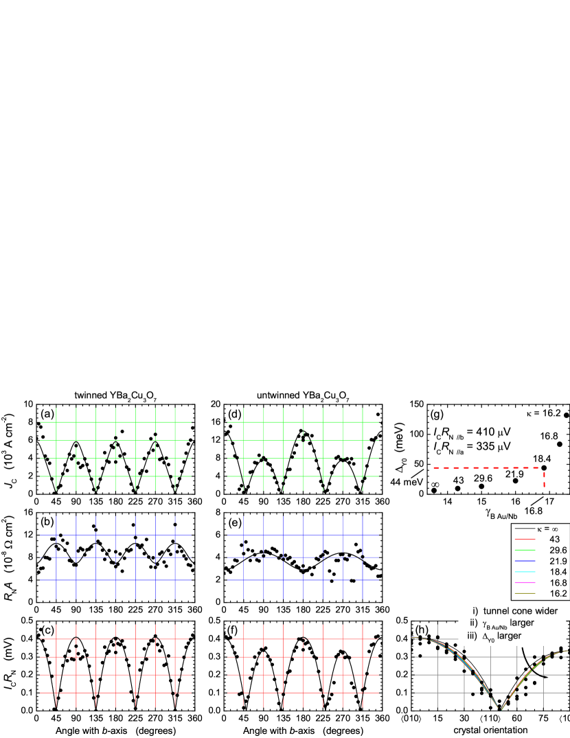
The suppressed in the nodal direction ( 0.01 suggests small, if not absent, imaginary admixtures, van:1995 for instance of isotropic -wave or -wave type which in contrast would lift the nodes. A significant real -wave admixture is excluded, because this would induce a rotation in the same direction with respect to the crystal of all nodes.
In the untwinned case, the -value is 1.8 times larger in the - than in the -direction. Preparation effects can be eliminated, since circular symmetry with respect to the substrate normal has been conserved at all phases of the fabrication. The normal-state resistance () is lower along the - than along the -axis, and presents a two-fold symmetry axis for the untwinned case. Using the angle-resolved values, the anisotropy in the -product amounts to .
To estimate the -products in our junctions, we model them as SINS’ structures, where S is YBa2Cu3O7, I is the YBa2Cu3O7/Au interface barrier, which has much higher resistance than the Au (N) and the Au/Nb (N/S’) interface. From independent resistance measurements on our PLD Au ( 4.6 cm at 4.2 K), the mean-free-path is 18 nm, and the dirty-limit coherence length is 49 nm. Using these values and the YBa2Cu3O7/Au interface resistance 10-8 cm2, the transparency at this interface is low: , where .Golubov:1995 From a small Fermi-velocity mismatch, we estimate the Au/Nb interface transparency much larger, 20. The electrode-separation is nm for nm thick Au and ramp angle . Since and , Au is in the diffusive regime, while YBa2Cu3O7 is in the clean limit with the anisotropic gap function .
We extend the expression for the supercurrent in diffusive SINS’ structures Golubov:1995 to our case of a low-transparent junction between a clean -wave superconductor and a diffusive NS’ bilayer. The contribution of midgap Andreev bound states is small in such a junction Riedel:1998 and can be neglected.
| (1) |
| (2) |
| (3) |
Here is the angle with the interface normal, and is the normalization constant. The integration is performed over angles to , and to of a half-sphere of all trajectories: for each junction orientation, and taking the crystal orientation and ramp-angle into account. The barrier transmission coefficient is in the limit of a small YBa2Cu3O7 Fermi velocity, where describes the tunnel-cone size. The sum in Eq.(2,3) is taken over the Matsubara frequencies . is the anisotropic gap function in YBa2Cu3O7, and is the isotropic proximity-induced gap function in Au. and are the bulk pair potential and the critical temperature of Nb, respectively. The critical current and -product should be found by calculating a maximum of over the phase difference across the junction.
Tunneling along the - and -axis may then be compared theoretically in terms of the ratio . Using Eqs.(1-3), it can be shown that for constant properties of the Nb/Au bilayer, the ratio of the YBa2Cu3O7 gap for these directions is . Therefore, the observed anisotropy of represents a lower limit for this gap ratio, which is valid for extremely small ratios . For increasing ratio the value requires a rapid increase of /. In this estimate, depends only on the gap ratios and on the Au/Nb interface transparency.
The anisotropic gap in YBa2Cu3O7 depends on the in-plane angle ( to ), and the angle (- to ) with the -plane. Various possible symmetry functions exist to describe this gap. Here, we consider the following 3D gap function in YBa2Cu3O7 consisting of a dominant -wave component with an isotropic and an anisotropic -wave admixture:
| (4) |
with the coefficients and . Here denotes the magnitude of the YBa2Cu3O7 gap at the interface. Consistent with our earlier estimate , the gap-ratio is taken as in agreement both with the observed node positions and ARPES.Aet:2001 With this, the coefficients are found from the fit to the data , and . Other choices for the gap symmetry functions lead to slightly different numbers but will not alter the basic results of our calculations.
A series of fits is presented in Fig. 3h: the wider the tunneling cone (smaller ), the smaller is the width of the oscillations in the -dependence (arrow). The effective YBa2Cu3O7 gap and must then become larger. This dependence is presented in Fig. 3g. The minimum value occurs for normal-incidence tunneling (, so that 6.4 meV. For reasonable values ( 0.5 eV), varies from 13.6 to about 18. This gives an estimate for the Au/Nb interface resistance: cm2. In contrast to , it is not possible to give an accurate estimate for the YBa2Cu3O7 gap from our data. Therefore, we choose to fit the data with meV, in Figs. 3c and 3f. These are not claimed to be the correct values; the simulation demonstrates however that large may well be consistent with small values. For the untwinned case , corresponding to a tunnel cone with a full-width-half-maximum (FWHM) of (cosine-term of not included). For the twinned case, the -dependence is simulated with the same parameters, except for a slightly smaller cone (, FWHM ), and assuming equal presence of both twin orientations: . The smaller tunnel cone for the twinned case is consistent with higher - and lower -values. This may result from a slightly thicker tunnel barrier at the YBa2Cu3O7/Au interface, e.g., due to minor variations in the Au PLD-conditions, modifying this interface.
The -dependence is fitted with an ellipsoidal relation of the conductivity projections along the main crystal directions of the YBa2Cu3O7. Written in terms of the -values along these directions, this gives . Fig. 3e shows the result using cm2 and cm2. For the twinned case, a geometrical average of the conductivities is assumed, . The used values in Fig. 3b read cm2, cm2. Although these phenomenological fits are indicative, angle-resolved calculations including aspects of the YBa2Cu3O7 band-structure and band-bending effects are needed for a detailed understanding. Finally, the fits are obtained with the ratios of the - and the -dependencies, the ensemble of which gives a consistent simulation of the angle-resolved junction properties.
The experimental results support theories based on a 2-band model of the chains and planes Mazin:1995 ; Donovan:1997 modeled with a symmetric, anti-symmetric and isotropic component. Furthermore, our findings agree with -axis tunneling from two twinned YBa2Cu3O7 grains to a Pb counter-electrode that depends on the magnetic field orientation,Kouznetsov:1997 and angle-dependence studies on grain boundary junctions.Lombardi:2002 For all-high- junctions and circuits, we mark the anisotropy as a possible intrinsic source of their limited reproducibility: both twin orientations may not be uniformly present, yielding an important variation in . Control over the crystal orientation then presents a key to improvement. Another important aspect concerns the nodes at from the crystal direction. The best choice for the electrode-orientation of devices aiming a -wave induced second harmonic in the current-phase relation, such as -SQUIDs based on grain boundary junctions, may therefore deviate from the crystal direction.
In conclusion, an angle-resolved electron tunneling study using Josephson junctions with an untwinned YBa2Cu3O7 base-electrode is presented. Evidence for significant in-plane anisotropy in the electronic properties of YBa2Cu3O7 is found.
The authors thank M. Yu. Kupriyanov, J. R. Kirtley, C. C. Tsuei, C. W. Schneider and J. Mannhart for valuable discussions. This work is supported by the Dutch Foundation for Research on Matter (FOM), and the Netherlands Organization for Scientific Research (NWO).
References
- (1) D. A. Wollmann et al., Phys. Rev. Lett. 71, 2134 (1993).
- (2) C. C. Tsuei et al., Phys. Rev. Lett. 73, 593 (1994).
- (3) J. Y. T. Wei et al., Phys. Rev. Lett. 81, 2542 (1998).
- (4) I. Maggio-Aprile et al., Phys. Rev. Lett. 75, 2754 (1995).
- (5) D. N. Basov et al., Phys. Rev. Lett. 74, 598 (1995)
- (6) A. G. Sun et al., Phys. Rev. B 52, R15731 (1995).
- (7) S. T. Johnson et al., Phys. Rev. Lett. 82, 2792 (1999).
- (8) T. Ishida et al., Physica C 263, 260 (1996).
- (9) K. Zhang et al., Phys. Rev. Lett. 73, 2484 (1994).
- (10) T. A. Friedmann et al., Phys. Rev. B 42, 6217 (1990).
- (11) M. F. Limonov et al., Phys. Rev. Lett. 80, 825 (1998).
- (12) H. Aubin et al., Phys. Rev. Lett. 78, 2624 (1997).
- (13) D. H. Lu et al., Phys. Rev. Lett. 86, 4370 (2001).
- (14) D. J. van Harlingen et al., Physica C 317-318, 410 (1999).
- (15) H. J. H. Smilde et al., Appl. Phys. Lett. 80, 4579 (2002).
- (16) J. M. Dekkers et al., Appl. Phys. Lett. 83, 5199 (2003).
- (17) M. Sigrist, T. M. Rice, J. Phys. Soc. Jpn. 61 , 4283 (1992).
- (18) D. J. van Harlingen, Rev. Mod. Phys. 67, 515 (1995).
- (19) A. A. Golubov et al., Phys. Rev. B 51, 1073 (1995).
- (20) R. A. Riedel, P. F. Bagwell, Phys. Rev. B 57, 6084 (1998).
- (21) I. I. Mazin, A. A. Golubov, A. D. Zaikin, Phys. Rev. Lett. 75, 2574 (1995).
- (22) C. O’Donovan et al., Phys. Rev. B 55 , 9088 (1997).
- (23) K. A. Kouznetsov et al., Phys. Rev. Lett. 79, 3050 (1997).
- (24) F. Lombardi et al., Phys. Rev. Lett 89, 207001 (2002).