CONSTRUCTION AND TESTS OF MODULES FOR THE ATLAS PIXEL DETECTOR
Abstract
The ATLAS Pixel Detector is the innermost layer of the ATLAS tracking system and will contribute significantly to the ATLAS track and vertex reconstruction. The detector consists of identical sensor-chip-hybrid modules, arranged in three barrels in the centre and three disks on either side for the forward region.
The position of the pixel detector near the interaction point requires excellent radiation hardness, mechanical and thermal robustness, good long-term stability, all combined with a low material budget. The pre-production phase of such pixel modules has nearly finished, yielding fully functional modules. Results are presented of tests with these modules.
1 Module Layout
A pixel module consists of a single n-on-n silicon sensor, approx. 26 cm2 in size. The sensor is subdivided into 47,268 pixels which are connected individually to 16 front-end (FE) chips via ”bumps”. These chips are connected to a module-control chip (MCC) mounted on a kapton-flex-hybrid glued onto the back-side of the sensor. The MCC communicates with the off-detector electronics via opto-links, whereas power is fed into the chips via cables connected to the flex-hybrid [1].
The sensor is subdivided into 41984 “standard” pixels of 50 m in azimuth times 400 m parallel to the LHC beam, and 5284 “long” pixels of m to cover the gaps between adjacent front-end chips. The module has 46080 read-out channels, which is smaller than the number of pixels because there is a 200 m gap in between FE chips on opposite sides of the module. To get full coverage the last eight pixels in each row are connected to only four channels (“ganged” pixels).
The connection between each pixel and its read-out channel is made through a bump bond. Two technologies are used, indium bumps and solder bumps. The minimum bump spacing is 50 m. No underfill material is used between the bumps to minimise the capacitive coupling between pixels as well as the capacitive load on the FE inputs. Consequently the bumped assembly is mechanically held together only by the bumps [2].
The FE chips contain 2880 individual charge sensitive analogue circuits with a digital read-out that operates at 40 MHz clock. The analogue part consists of a high-gain, fast preamplifier followed by a DC-coupled second stage and a differential discriminator. The threshold of the discriminator ranges up to 1 fC, its nominal value being 0.5 fC. On top of a globally set threshold value the threshold of each of the 2880 channels can be adjusted individually to allow fine tuning. When a hit is detected by the discriminator the pixel address and the time at which the hit occured is provided. Alongside that the time over threshold (ToT) information allows reconstruction of the charge seen by the preamplifier. The pixel address and timing/charge information is then passed to buffers at the bottom of the chip where data waits for a matching trigger before being sent to the MCC. The MCC does a first event-building of the individual data of the 16 FE chips [3].
2 Module Tests
In order to assure full functionality of the modules in the later experiment, measurements in a test beam and at the production sites are performed.
Beam tests are performed at the SPS at CERN using 180 GeV/c hadrons. The setup consists of a beam telescope for the position measurement [4], trigger scintillators for timing measurement to 36 ps, and up to four pixel modules. The number of defective channels is observed to less than and for standard pixels the efficiency for normal incidence particles is 99.570.15%. The timewalk, i.e. the variation in the time when the discriminator input goes above threshold, is an issue since hits with a low deposited charge have an arrival time later than the ones with high charges, in particular for ganged pixels. This problem has been addressed in the latest version of FE chips.
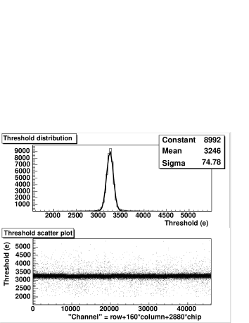
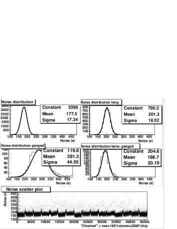
An important test that allows a large range of in-laboratory measurements is the threshold scan. Signals are created with on-module charge injection and scanning the number of hits versus the so injected charge yields the physical value of the threshold of the discriminator and the equivalent noise charge as seen by the preamplifier. A set of such scans is used to reduce the threshold dispersion by adjusting a parameter individually for each channel (see above). The resulting threshold and noise after threshold tuning is shown in figure 1. Typically approx. 100 e threshold dispersion across a module and a noise value of below 200 e for standard pixels is achieved, as is needed for good performance.
In a similar fashion, the cross-talk is measured to a few per cent for standard pixels and a timewalk measurement yields a result similar to that from the test beam. Data taken when illuminating the sensor with a radioactive source allows in-laboratory detection of defective channels, again yielding a number similar to that of the test beam. The source-spectrum reconstructed from the ToT-readings is in agreement with expectations.
In addition, modules are irradiated to a dose approximately corresponding to 10 years of ATLAS operation The latter results are currently only preliminary and are thus not reported here although they look promising.
References
- [1] A. Andreazza et al., ATLAS EDMS-note ATL-IP-AN-0002 (2002).
- [2] R. Boyd et al., ATLAS EDMS-note ATL-IP-AN-0003 (2002).
- [3] R. Beccherle et al., Nuclear Instr. Meth. A 492, 117 (2002).
- [4] J. Treis et al., Nuclear Instum. Meth. A 490, 112 (2002).