Transport through a strongly coupled graphene quantum dot in perpendicular magnetic field
Abstract
We present transport measurements on a strongly coupled graphene quantum dot in a perpendicular magnetic field. The device consists of an etched single-layer graphene flake with two narrow constrictions separating a 140 nm diameter island from source and drain graphene contacts. Lateral graphene gates are used to electrostatically tune the device. Measurements of Coulomb resonances, including constriction resonances and Coulomb diamonds prove the functionality of the graphene quantum dot with a charging energy of meV. We show the evolution of Coulomb resonances as a function of perpendicular magnetic field, which provides indications of the formation of the graphene specific Landau level. Finally, we demonstrate that the complex pattern superimposing the quantum dot energy spectra is due to the formation of additional localized states with increasing magnetic field.
I Introduction
Graphene nov04 ; gei07 , a two-dimensional solid consisting of carbon atoms arranged in a honeycomb lattice has a number of unique electronic properties cas09 such as the gapless linear dispersion, and the unique Landau level (LL) spectrum nov05 ; zha05 . The low atomic weight of carbon and the low nuclear spin concentration, arising from the % natural abundance of 12C, promises weak spin orbit and hyperfine coupling. This makes graphene a promising material for spintronic devices Awsch07 ; Tomb07 and spin-qubit based quantum computation Loss98 ; Elzer04 ; Petta05 ; Trau07 . Additionaly, the strong suppression of electron backscattering nov05 ; zha05 makes it interesting for future high mobility nanoelectronic applications in general kat07 ; Avouris07 . Advances in fabricating graphene nanostructures have helped to overcome intrinsic difficulties in (i) creating tunneling barriers and (ii) confining electrons in bulk graphene, where transport is dominated by Klein tunneling-related phenomena dom99 ; kat06 . Along this route graphene nanoribbons han07 ; che07 ; dai08 ; sta09 ; mol09 ; tod09 ; liu09 and quantum dots sta08a ; pon08 ; sta08aa ; sch09 ; gue09 ; gue09a ; gue08 ; ihn10 have been fabricated. Coulomb blockade sta08a ; pon08 ; sta08aa , quantum confinement effects sch09 ; gue09 ; gue09a and charge detection gue08 have been reported. Moreover, graphene nanostructures may allow to investigate phenomena related to massless Dirac Fermions in confined dimensions pon08 ; ber87 ; sch08 ; rec09 ; lib10 ; lib09 ; you09 . In general, the investigation of signatures of graphene-specific properties in quantum dots is of interest to understand the addition spectra, the spin states and dynamics of confined graphene quasi-particles.
Here, we report on tunneling spectroscopy (i.e. transport) measurements on a 140 nm graphene quantum dot with open barriers, which can be tuned by a number of lateral graphene gates mol07 . In contrast to the measurements reported in Ref. gue09, the more open dot in the present investigation enables us to observe Coulomb peaks with higher conductance and the larger dot size reduces the magnetic field required to see graphene specific signatures in the spectra. We characterize the graphene quantum dot device focusing on the quantum dot Coulomb resonances which can be distinguished from additional resonances present in the graphene tunneling barriers. We discuss the evolution of a number of Coulomb resonances in the vicinity of the charge neutrality point in a perpendicular magnetic field from the low-field regime to the regime where Landau levels are expected to form. In particular, we investigate the device characteristics at elevated perpendicular magnetic fields, where we observe the formation of multiple-dots giving rise to (highly reproducible) complex patterns in the addition spectra.
II Device fabrication
The fabrication process of the presented graphene nano-device is based on the mechanical exfoliation of (natural) graphite by adhesive tapes [24, 25, 28]. The substrate material consists of highly doped silicon (Si++) bulk material covered with 295 nm of silicon oxide (SiO2), where thickness (and roughness) of the SiO2 top layer is crucial for the Raman dav07a and scanning force microscope based identification of single-layer graphene flakes. Standard photolithography followed by metalization and lift-off is used to pattern arrays of reference alignment markers on the substrate which are later used to re-identify the locations of individual graphene flakes on the chip and to align further processing patterns. The graphene flakes are structured to submicron dimensions by electron beam lithography (EBL) and reactive ion etching based techniques in order to fulfill the nanodevice design requirement.
After etching and removing the residual resist, the graphene nanostructures are contacted by an additional EBL step, followed by metalization and lift-off.
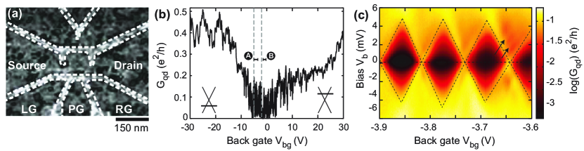
A scanning force microscope image of the final device studied here is shown in Fig. 1a. The approximately 140 nm diameter graphene quantum dot is connected to source (S) and drain (D) via two graphene constrictions with a width of nm and a length of nm, both acting as tunneling barriers. The dot and the leads can be further tuned by the highly doped silicon substrate used as a back gate (BG) and three in-plane graphene gates: the left side gate (LG), the plunger gate (PG) and the right side gate (RG). Apart from the geometry, the main difference of this sample compared to the device presented in Ref. gue09, is the higher root mean square variation of the height () on the island. While there are no visible resist residues on the island of the sample in Ref. gue09, with nm, there are many dot-like residues on the sample presented here giving nm.
III Measurements
All measurements have been performed at a base temperature of T = 1.8 K in a variable temperature cryostat. We have measured the two-terminal conductance through the graphene quantum dot device by applying a symmetric DC bias voltage while measuring the source-drain current through the quantum dot with a noise level below 10 fA. For differential conductance measurements a small AC bias, 100 V has been superimposed on and the differential conductance has been measured with lock-in techniques at a frequency of 76 Hz.
In Fig. 1b we show the conductance as a function of back gate voltage at low bias ( = 200 V) highlighting the strong suppression of the conductance around the charge neutrality point (-5 3 V) due to the so-called transport gap tod09 ; sta09 ; mol09 ; liu09 . Here we tune transport from the hole to the electron regime, as illustrated by the left and right inset in Fig. 1b. The large number of resonances with amplitudes in the range of up to inside the gap region may be due to both, (i) resonances in the graphene constrictions acting as tunneling barriers [4] (and thus being mainly responsible for the large extension of this transport gap) and (ii) Coulomb resonances of the quantum dot itself (see also examples of Coulomb diamonds in Fig. 1c). At room temperature these resonances disappear and a conductance value of is measured at = 0 V.
III.1 Coulomb blockade measurements at B = 0 T
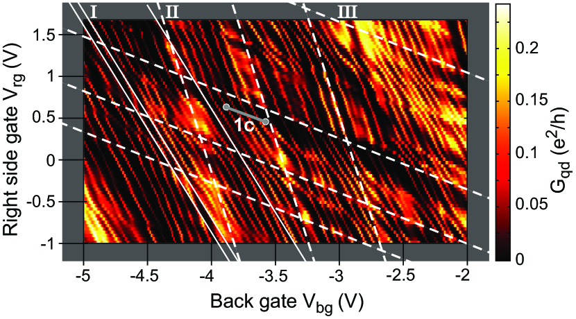
By focusing on a smaller back gate voltage range within the transport gap (indicated by the dashed lines in Fig. 1b) and measuring the conductance as a function of and the right side gate much more fine-structure appears, as shown in Fig. 2. A large number of resonances is observed with sequences of diagonal lines (see white lines in Fig. 2) with different slopes, corresponding to different lever arms (’s). By sweeping the right side gate () we break the left-right symmetry of the transport response (see also Fig. 1a). This allows us to distinguish between resonances located either near the quantum dot or the left and right constriction. The steeper the slope in Fig. 2 the less this resonance can be electrostatically tuned by the right side gate and, consequently, the larger the distance between the corresponding localized state and the right side gate. Subsequently, the steepest slope (II, corresponding to = 0.2) can be attributed to resonances in the left constriction and the least steepest slope (III, = 1.6) belongs to resonances in the right constriction. Both are highlighted as white dashed lines in Fig. 2. The Coulomb resonances of the quantum dot appear with an intermediate slope (I, = 0.4) and exhibit clearly the smallest spacing in back gate voltage, 0.1 V. This is a good indication that they belong to the largest charged island in the system, which obviously is the 140 nm large graphene quantum dot, which is much larger than the localized states inside the graphene constrictions acting as tunneling barriers.
Corresponding Coulomb diamond measurements kou97 , that is, measurements of the differential conductance as a function of bias voltage and (i.e. V) have been performed along the (diagonal) solid gray line in Fig. 2 and are shown in Fig. 1c. From the extent of these diamonds in bias direction we estimate the average charging energy of the graphene quantum dot to be meV, which is in reasonable agreement with the size of the graphene quantum dot sta08a ; sta08aa ; sch09 . Moreover, we observe faint strongly broadened lines outside the diamonds running parallel to their edges, as indicated by arrows in Fig. 1c. The extracted energy difference of roughly 1 meV is reasonable for electronic excited states in this system sch09 .
III.2 Coulomb resonances as a function of a perpendicular magnetic field
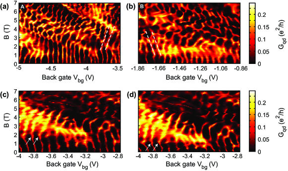
In Fig. 3 we show a large number of Coulomb resonances as function of a magnetic field perpendicular to the graphene sample plane. The measurement shown in Fig. 3a has been taken in the back gate voltage range from -5 to -3.5 V, at V (highlighted by the horizontal line (A) in Fig. 1b). Thus we are in a regime where transport is dominated by holes (i.e. we are at the left hand side of the charge neutrality point in Fig. 1b), which is also confirmed by the evolution of the Coulomb resonances in the perpendicular magnetic field as shown in Fig. 3a. There is a common trend of the resonances to bend towards higher energies (higher ) for increasing magnetic field, in good agreement with Refs. gue09 ; gue09a ; sch08 ; rec09 ; lib10 . The finite magnetic field introduces an additional length scale nm which competes with the diameter of the dot. Therefore the ratio is a relevant parameter for the observation of Landau levels in graphene quantum dot devices. Here, the comparatively large size ( 140 nm) of the dot promises an increased spectroscopy window for studying the onset and the formation of Landau levels in graphene quantum dots in contrast to earlier work gue09 ; gue09a (where 50 nm). Moreover, we expect that in larger graphene quantum dots, where the surface-to-boundary ratio increases edge effects should be less relevant. In Figs. 3a,c,d we indeed observe some characteristics of the Fock-Darwin-like spectrum sch08 ; rec09 ; lib10 of hole states in a graphene quantum dot in the near vicinity of the charge neutrality point: (i) the levels stay more or less at constant energy (gate voltage) up to a certain B-field, where (ii) the levels feature a kink, whose B-field onset increases for increasing number of particles, and (iii) we observe that the levels convergence towards higher energies (see white dashed lines in Fig. 3a). The pronounced kink feature (see arrows in Figs. 3c,d) indicate filling factor = 2 in the quantum dot. However, this overall pattern is heavily disturbed by additional resonances caused by localized states, regions of multi-dot behavior, strong amplitude modulations due to constriction resonances and a large number of additional crossings, which are not yet fully understood. This becomes even worse when investigating the electron regime (see horizontal line (B) in Fig. 1b), as shown in Fig. 3b. Individual Coulomb resonances can (only) be identified for low magnetic fields B 2 T and a slight tendency for their bending towards lower energies might be identified (please see white dashed lines in Fig. 3b). For magnetic fields larger than 3 T it becomes very hard to identify individual Coulomb resonances in the complex and reproducible conductance pattern.
In order to demonstrate the reproducibility of these complex patterns we show an up (Fig. 3c) and a down (Fig. 3d) sweep of the very same - parameter space. These two measurements, have different resolution and thus different sweep rates in both the and direction. However, all the individual features are highly reproducible (but hard to understand) despite the fact that we find some small hysteresis in magnetic field for T (see white arrows in Figs. 3c,d). The origin of the complex patterns shown in Fig. 3 can be understood when having a closer look at charge stability diagrams (such as Fig. 2) for different magnetic fields.
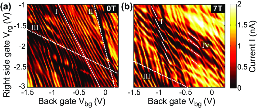
In Fig. 4a we show an example of a sequence of dot Coulomb resonances in the - plane. The slope corresponding to and the spacing of V are in good agreement with Fig. 2 and lead to the conclusion that we observe single quantum dot behavior over a large parameter range. However, if we measure the current in the very same - parameter space at B = 7 T the pattern changes significantly and the diagonal lines are substituted by a strong hexagonal pattern (see dashed lines) typical for two coupled quantum dots wiel02 . The two states forming the hexagone pattern show relative lever arms of and . While the resonances with are attributed to the original dot, corresponds to a new and strongly coupled localization formed close to the right constriction. Additional resonances from the right constriction with (see above) are still visible.
We interpret the magnetic field dependence in the following way. At low but increasing magnetic field we see in almost all measurements an increase of the conductance through the dot (see e.g. Fig. 3). Assuming diffusive boundary scattering such a conductance onset in magnetic field occurs due to reduced backscattering bvh91 and has been observed in other measurements on graphene nanoribbons oost10 ; bai10 . The maximum conductance is reached around T corresponding to a magnetic length nm in rough agreement with the size of the constriction. As the magnetic field is further increased the complex pattern with many crossings starts to emerge, attributed to the formation of additional quantum dots around the right constriction with strong coupling to the original dot. The formation of such localized puddles is understood as a consequence of the increased magnetic confinement where is getting smaller than the extension of potential valleys induced by disorder.
IV Conclusion
In summary we have presented detailed studies of transport through an open and larger graphene quantum dot (compared to Ref. gue09, ) in the vicinity of the charge neutrality point as a function of perpendicular magnetic field. The evolution of Coulomb resonances in a magnetic field showed the signatures of Landau level formation in the quantum dot. Indications for the crossing of filling factor = 2 are obtained by the observation of kinks in spectral lines before bending towards the charge neutrality point. However the observation is disturbed by the formation of a pronounced additional localized state at high magnetic fields in the vicinity of the right constriction. Although the use of open constrictions enhances the visibility of the Coulomb peaks and reduces the transport-gap region, emerging pronounced parasitic localized states make the analysis very difficult. For a further in-depth analysis of the addition spectra around the electron-hole crossover it is hence beneficial to minimize the amount of disorder and to use clearly defined constrictions. These should be thin compared to the dot diameter in order to get different energy scales for quantum dot resonances and constriction resonances, which are easy to distinguish. However, the constrictions need to be wide enough to enable conductance measurements around the electron-hole crossover without a charge detector.
Acknowledgment — The authors wish to thank F. Libisch, P. Studerus, C. Barengo, F. Molitor and S. Schnez for help and discussions. Support by the ETH FIRST Lab, the Swiss National Science Foundation and NCCR nanoscience are gratefully acknowledged.
References
- (1) K. S. Novoselov, A. K. Geim, S. V. Morozov, D. Jiang, M. I. Katsnelson, S. V. Dubonos, I. V. Grigorieva, and A. A. Firsov, Science 306, 666, (2004)
- (2) For review see e.g.: A. K. Geim and K. S. Novoselov, Nat. Mater. 6, 183 (2007)
- (3) A. H. Castro Neto, F. Guinea, N. M. R. Peres, K. S. Novoselov, and A.K. Geim, Rev. Mod. Phys. 81, 109 (2009)
- (4) K. S. Novoselov, A. K. Geim, S. V. Morozov, D. Jiang, M. I. Katsnelson, I. V. Grigorieva, S. V. Dubonos, A. A. Firsov, Nature 438, 197-200, (2005)
- (5) Y. Zhang, Y.-W. Tan, H. L. Stormer, P. Kim, Nature 438, 201-204, (2005)
- (6) D. D. Awschalom and M. E. Flatt , Nature Physics 3, 153, (2007)
- (7) N. Tombros, C. Jozsa, M. Popinciuc, H. T. Jonkman and B. J. van Wees, Nature 448, 571, (2007)
- (8) D. Loss and D. P. DiVincenzo, Phys. Rev. A. 57, 120, (1998)
- (9) J. M. Elzerman, R. Hanson, L. H. Willems van Beveren, B. Witkamp, L. M. K. Vandersypen and L. P. Kouwenhoven, Nature 430, 431 (2004)
- (10) J. R. Petta, et al., Science 309, 2180, (2005)
- (11) B. Trauzettel, D. V. Bulaev, D. Loss and G. Burkard, Nature Phys. 3, 192, (2007)
- (12) M. I. Katnelson, Materials Today 10(1-2), pp. 20-27, (2007)
- (13) P. Avouris, Z. H. Chen, V. Perebeinos, Nature Nanotechnology 2, 605, (2007)
- (14) N. Dombay, and A. Calogeracos, Phys. Rep. 315, 41 58 (1999)
- (15) M. I. Katsnelson, K. S. Novoselov, amd A. K. Geim, Nature Phys. 2, 620 625 (2006)
- (16) M. Y. Han, B. Özyilmaz, Y. Zhang, and P. Kim, Phys. Rev. Lett. 98, 206805 (2007)
- (17) Z. Chen, Y.-M. Lin, M. Rooks and P. Avouris, Physica E 40, 228, (2007)
- (18) X. Li, X. Wang, L. Zhang, S. Lee, H. Dai, Science 319, 1229 (2008)
- (19) C. Stampfer, J. Güttinger, S. Hellmüller, F. Molitor, K. Ensslin, and T. Ihn, Phys. Rev. Lett. 102, 056403 (2009)
- (20) F. Molitor, A. Jacobsen, C. Stampfer, J. Güttinger, T. Ihn, and K. Ensslin, Phys. Rev. B 79, 075426 (2009)
- (21) K. Todd et al., Nano Lett. 9, 416 (2009)
- (22) X. Liu, J. Oostinga, A. F. Morpurgo, and L. M. K. Vandersypen, Phys. Rev. B, 80, 121407(R), (2009)
- (23) C. Stampfer, J. Güttinger, F. Molitor, D. Graf, T. Ihn, and K. Ensslin, Appl. Phys. Lett. 92, 012102 (2008)
- (24) L. A. Ponomarenko, F. Schedin, M. I. Katsnelson, R. Yang, E. H. Hill, K. S. Novoselov, and A. K. Geim, Science 320, 356 (2008)
- (25) C. Stampfer, E. Schurtenberger, F. Molitor, J. Güttinger, T. Ihn, and K. Ensslin, Nano Lett. 8, 2378 (2008)
- (26) S. Schnez, F. Molitor, C. Stampfer, J. Güttinger, I. Shorubalko, T. Ihn, and K. Ensslin, Appl. Phys. Lett. 94, 012107 (2009)
- (27) J. Güttinger, C. Stampfer, F. Libisch, T. Frey, J. Burgdörfer, T. Ihn and K. Ensslin, Phys. Rev. Lett. 103, 046810 (2009)
- (28) J. Güttinger, C. Stampfer, T. Frey, T. Ihn, and K. Ensslin, Phys. Status Solidi 246, 2553 (2009)
- (29) J. Güttinger, C. Stampfer, S. Hellmüller, F. Molitor, T. Ihn, and K. Ensslin, Appl. Phys. Lett. 93, 212102 (2008)
- (30) For a review on graphene single electron transistors: T. Ihn, J. Güttinger, F. Molitor, S. Schnez, E. Schurtenberger, A. Jacobsen, S. Hellmüller, T. Frey, S. Dröscher, C. Stampfer, and K. Ensslin, Materials Today 13, 44 (2010)
- (31) M. V. Berry and R. J. Mondragon, Proceedings of the Royal Society of London A 412, 53-74 (1987)
- (32) S. Schnez, K. Ensslin, M. Sigrist, and T. Ihn, Phys. Rev. B 78, 195427 (2008)
- (33) P. Recher, J. Nilsson, G. Burkard, and B. Trauzettel, Phys. Rev. B 79, 085407 (2009)
- (34) F. Libisch, S. Rotter, J. Güttinger, C. Stampfer, K. Ensslin and J. Burgdörfer, Phys. Rev. B 81, 245411 (2010)
- (35) F. Libisch, C. Stampfer, and J. Burgdörfer, Phys. Rev. B 79, 115423 (2009)
- (36) A. F. Young and P. Kim, Nature Phys. 5, 222-226 (2009)
- (37) F. Molitor, J. Güttinger, C. Stampfer, D. Graf, T. Ihn, and K. Ensslin, Phys. Rev. B 76, 245426 (2007)
- (38) D. Graf, F. Molitor, K. Ensslin, C. Stampfer, A. Jungen, C. Hierold and L. Wirtz Nano Lett. 7 238 (2007)
- (39) L. P. Kouwenhoven et al., 1997 Electron transport in quantum dots (Mesoscopic Electron Transport ed L. L. Sohn, L. P. Kouwenhoven and G. Schön (Dotrecht: NATO Series, Kluwer)
- (40) W. G. van der Wiel, S. De Franceschi, J. M. Elzerman, T. Fujisawa, S. Tarucha, and L. P. Kouwenhoven, Rev. Mod. Phys. 75, 1 (2002)
- (41) C. W. J. Beenakker and H. van Houten, in Solid State Physics, edited by H. Ehrenreich and D. Turnbull (Academic, New York, 1991), Vol. 44, p. 15.
- (42) J.B. Oostinga, B. Sac p , M. F. Craciun, and A. F. Morpurgo Phys. Rev. B 81, 193408 (2010)
- (43) J. Bai, R. Cheng, F. Xiu, L. Liao, M. Wang, A. Shailos, K. L. Wang, Y. Huang, and X. Duan, Nature Nanotech. doi:10.1038/nnano.2010.154 (2010)