Influence of electron scatterings on thermoelectric effect
Abstract
In this work, we employed non-equilibrium Green’s function to investigate the electron transport properties in the nanowire with the presence of scatterings. The scattering mechanism is modelled by using the concept of Büttiker probe. The effect of electron scattering is analyzed under three conditions: absence of external field; with a bias voltage; and with a finite temperature difference. It is found weak and strong scatterings strength affect the electron transport in different ways. In the case of weak scattering strength, electron trapping increase the electron density, hereafter boost the conductance significantly. Although the increment in conductance would reduce the Seebeck coefficient slightly, the power factor still increases. In the case of strong scattering strength, electron diffraction causes the redistribution of electrons, accumulation of electron at the ends of the wire blocks current flow; hence the conductance is reduced significantly. Although the Seebeck coefficient increases slightly, the power factor still decreases. The power factor is enhanced by , at the optimum scattering strength.
pacs:
PACS numberyear number number identifier Date text]date
LABEL:FirstPage1 LABEL:LastPage#12
I Introduction
Thermoelectric (TE) device is a type of green energy devices and is of great possibility to be used widely in near future. Currently, the limitation of TE device is its low energy conversion efficiency, and has attracted much attention Science1999 ; Nature2001 ; Science2002 ; Science2004 ; Nature2008YangPD ; 159Nature2008 ; Ali . The efficiency of a TE device is indicated by the dimensionless TE figure of merit (), determined by the expression using its parameters Seebeck coefficient , electric conductivity , thermal conductivity (, contributed by electrons and phonons) and the temperature . Among these parameters, , and are related to the electron transport and is related to the phonon transport. Therefore, the strategies of developing high device are improving the electronic TE efficiency and reducing the lattice thermal conductivityLJTE . Currently, most of the efforts are put in to reduce the lattice thermal conductivity by investigation the phonon transport, which can be found in our previous works LJ1 ; LJ2 ; Zhao . However, more attentions needs to be paid on the electron transport, as the electronic TE efficiency limits the performance of TE device significantlyLJTE . The best TE device has a Dirac delta shaped electron transmission functionMahan 1996 . Besides the TE efficiency, the power factor (), related to the power rating, is another important index of TE device.
In nano-scaled device, the concept of ballistic transport of electrons is important. However, electron scatterings still occurs for the reason of defects, grain boundaries, phonons, and charges in the device. Electron scatterings affect the transport properties, and further influence the TE effect of the device. A previous work has studied the effect of nano-particle scattering on TE power factorMona . It is found that the electron concentration is usually higher in the sample with nano-particles, implying the Seebeck coefficient is usually unchanged and conductivity is increased at the optimum of the power factor. That work is based on low nano-particle concentration, and that work rise our interest in the problem of the electron scattering strength on TE effect. In this work, we employed non-equilibrium Green’s function to investigate the electron transport properties in nanowire with the presence of electron scatterings. Scattering points are inserted into the nanowire, and are modelled by Büttiker probesDatta2003 . The response of the device to an external field, due to a temperature difference or a bias voltage, is discussed with a wide range of scattering strength.
II Theory
A silicon nanowire with square cross-sectional shape coupled by two contacts, which are served as thermal and electric reservoirs, is considered as shown in Fig.1. The wire is composed of many slices with the thickness () nm parallel to the contact interface. For the slice at position , the effective potential is given by
| (1) |
The variables is the quantum number for the energy in transverse direction; the side length of the cross-section (set to nm in the computation); the electric potential energy; the effective mass of silicon; and the Dirac constant. The Hamiltonian of the wire for the mode, denoted by the subscript (), is constructed as follow:
| (2) |
where is the coupling energy between two slices determined by the expression (about meV in this model).
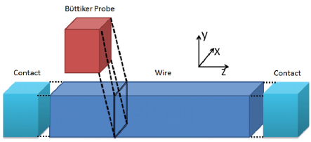
To reveal the effect of the electron scattering, the scattering points modelled by Büttiker probes are inserted into the wire. At a scattering point, the slice of the wire is coupled to the Büttiker probe with the coupling strength (), as shown in Fig.1. The coupling strength determines the electron scatterings strength. For the convenience in discussion, we define the scattering factor , the relative scattering strength respected to the coupling strength between two slices. Hence , and equal to is equivalent to the thermal energy at K, which is about meV.
All the contacts in the system, including both virtual contacts (Büttiker probes) and two real contacts, are labeled by index . The self-energy due to the contact is given by
| (3) |
where is the longitudinal wave vector determined by
| (4) |
The broadening function of the contact is then obtained from its self-energy:
| (5) |
The total self-energy of the wire is the sum of the contribution from each contact. The retarded and advanced Green’s function of the wire, and , are then determined by:
| (6) | ||||
| (7) |
where is an infinitesimal positive number. With that, the electron transmission function between contact and contact is given by
| (8) |
The electric current of contact is determined by the Landauer-Büttiker formula:
| (9) |
where is the Fermi-Dirac distribution at contact with the Fermi level , defined by
| (10) |
To fulfill the charge conservation, the net current of each Büttiker probe is set to zero by adjusting the Fermi levels of Büttiker probes using Jacobian method, (linear temperature gradient is assumed in the wire). The Fermi levels in the left and right contacts are determined by assuming all donors are ionized, and the donor concentration cm-3 is used in the computation. The number of electrons in each slices of the wire are obtained from the diagonal elements of , determined by the following expression:
| (11) |
The potential energy for each slice is updated by the Poisson equation using the electron density determined by the above formula, and the final status of the system is obtained after the self-consistent iteration process.
III Discussion
In the following, the system at room temperature in three conditions: (A) absence of external field, (B) with a bias voltage, and (C) with a finite temperature difference, are discussed.
III.1 Absence of external field: electron trapping and diffraction
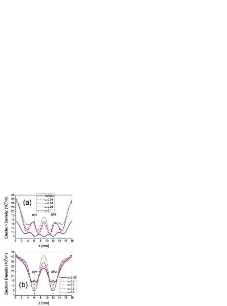
In this section, the length of the nanowire is set to nm, and two scattering points are inserted at the positions of nm and nm. With the absence of external field, i.e. both temperatures and voltages at the two contacts are equal, the electron charge density along the wire determined by Green’s function is shown in Fig.2, in which the scattering points are denoted by “SP1” and “SP2”. In the case of ballistic transport (), electron scattering only occurs at the contact interfaces, but not in the wire. For this reason, electrons are accumulated at both ends of the wire, that incur the repulsion of electron as the result of the Coulomb force. Therefore, a fluctuation of electron density is observed in the wire, as shown by the “Ballistic” curve in Fig.2a. When the scattering strength getting slightly stronger (), the electron wave function in the wire is reconstructed due to the perturbation of the scattering points, but this effect is not significant. Electron scattering occurs when electron collide with the scattering points, and electrons are accumulated in the wire. Fig.2a shows the stronger scattering strength, the more electrons are trapped inside the wire, especially near the scattering points in the weak scattering strength region (). This result is consistent with the previous workMona . However, in strong scattering strength region, this effect vanished. This is because the electron wave function is significantly modified by the scattering points. The probability of finding an electron near the scattering points become much smaller, therefore the electron density near scattering points reduces (Fig.2b), the chance of electron scatterings decreases, the chance of electron scatterings decreases. This phenomenon is known as the electron diffraction, electrons prefer avoiding the scattering points than being scattered.
III.2
A bias voltage
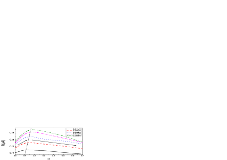
In the following, we discussed a nm nanowire at room temperature with a bias voltage. A single scattering point is considered at the center of the wire. In the case of ballistic transport (), due to the external field, electron density is tilting toward one end of the wire, as shown in Fig.3a. With slightly increases in the scattering strength, more electrons are accumulated in the wire, especially near the scattering point. This is consistent with the discussion in section A. With the bias voltage, the increment in electron density is conducive to boost the electric current as shown by Fig.3b. However, in strong scattering strength region, electrons are bypassing the scattering point by reconstructing their wave functions. This leads to the accumulation of electrons near the contact interfaces (Fig.3c), which block current flow. So, decrease in electric current is expected (see Fig.3d).
With different bias voltages, the electric current respect to the scattering strength are in the similar profile: a rise followed by a drop (Fig.4). Also, the scattering strength at which the maximum current occurs, increases with the bias voltage. This phenomenon can be understood in the following way. The electrons are trapped in the wire in the weak scattering strength region. With the increase in the bias voltage, these electrons can be accelerated and contribute to the electric current. Higher bise voltage has stronger power in accelerating electron, therefore the scattering strength at which the maximum current occurs is increasing with the bias voltage. With sufficiently large scattering strength, the diffraction of electron causes the accumulation of electrons at both ends of the wire, which blocks the electric current.
III.3 A finite temperature difference
To discussion the TE effect, a nm nanowire under a temperature difference is considered. The temperature difference is split into half and applied to the contacts, i.e. and . In general, TE effect is evaluated in the open circuit condition. Therefore, the net current is zero. For this reason, to offset the current produced by the temperature difference, an electric field is generated. The ratio of the voltage difference over the temperature difference gives the Seebeck coefficient. To determine the conductance of the wire in the presence of temperature difference, a testing current (a small current) is injected into the wire. From the change of the voltage difference, the conductance is obtained.
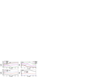
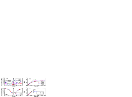
In the weak scattering strength region (), Seebeck coefficient is smaller with stronger scattering. That is because the electric conductance increases (Fig.5b), and a smaller electric field is sufficient enough to offset the current produced by temperature difference for case of larger conductance. Similarly, in the strong scattering strength region, Seebeck coefficient increases as the result of the decrease in the electric conductance, as shown in Fig.5c and Fig.5d.
In Fig.5b, the conductance increases with the temperature difference, and starts to decrease after the critical temperature difference, also the critical temperature difference increases with the scattering strength. This is because, when temperature difference is small, the increment in temperature difference intends to inject more electrons into the wire; these electrons are trapped easily by the scattering point, lead to the a higher electron density and a larger conductance. When the temperature difference is more than the critical value, more electrons are injected than the wire could conduct, that causes the redistribution of electrons, which limits current flow. Due to this effect on conductance, Seebeck coefficient decreases at first and start to increase after the critical temperature difference (Fig.5a). In the strong scattering strength region, the fluctuations in conductance and Seebeck coefficient are not as much as that in weak scattering strength region. This is because the chance of electron scatterings is reduced due to the effect of electron diffraction, number of electrons trapped in the wire is smaller than the case of weak scattering strength.
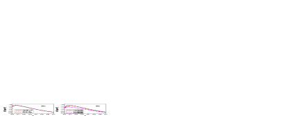
Fig.6 shows the TE power factors with the change of scattering strength. The power factor has maximum value at about , and it drops dramatically after that. The explanation of the change in power factor can be ascribed to the change in the the conductance and Seebeck coefficient. At the optimum power factor (), comparing to the ballistic case, for equals to K, K and K, the Seebeck coefficient drops by , and (Fig.5a); but the conductance increases by , and (Fig.5b), therefore the power factor is increased by , and , respectively. Due to the shifting of the critical temperature difference mentioned in previous paragraph, the power factor has the maximum enhancement when the temperature difference is about K.
IV Conclusion
Weak and strong scatterings strength affect the electron transport in different manners. In the case of weak scattering strength, electron trapping increase the electron density, boost the conductance significantly. The increment in conductance would reduce the Seebeck coefficient slightly, but overall the power factor increases. In the case of strong scattering strength, electron diffraction causes the redistribution of electrons, accumulation of electrons at the ends of the wire block current flow, hence the conductance is suppressed significantly. Due to this effect, the Seebeck coefficient increases slightly, but the power factor decreases severely.
References
- (1) Francis J. DiSalvo, Science 285, 703 (1999).
- (2) Rama Venkatasubramanian, Edward Siivola, Thomas Colpitts, and Brooks O’Quinn, Nature 413, 597 (2001).
- (3) T. C. Harman, P. J. Taylor, M. P. Walsh, and B. E. LaForge, Science 297, 2229 (2002).
- (4) Kuei Fang Hsu, Sim Loo, Fu Guo, Wei Chen, Jeffrey S. Dyck, Ctirad Uher, Tim Hogan, E. K. Polychroniadis, and Mercouri G. Kanatzidis, Science 303, 818 (2004).
- (5) Allon I. Hochbaum, Renkun Chen, Raul Diaz Delgado, Wenjie Liang, Erik C. Garnett, Mark Najarian, Arun Majumdar, and Peidong Yang, Nature 451, 163 (2008).
- (6) Akram I. Boukai, Yuri Bunimovich, Jamil Tahir-Kheli, Jen-Kan Yu, William A. Goddard Iii, and James R. Heath, Nature 451, 168 (2008).
- (7) Sebastian Volz, Ali Shakouri, and Mona Zebarjadi, in Thermal Nanosystems and Nanomaterials (Springer Berlin / Heidelberg, 2009), Vol. 118, pp. 225.
- (8) G. D. Mahan and J. O. Sofo, Proceedings of the National Academy of Sciences 93, 7436 (1996).
- (9) Mona Zebarjadi, Keivan Esfarjani, Ali Shakouri, Je-Hyeong Bahk, Zhixi Bian, Gehong Zeng, John Bowers, Hong Lu, Joshua Zide, and Art Gossard, Applied Physics Letters 94, 202105 (2009).
- (10) R. Venugopal, M. Paulsson, S. Goasguen, S. Datta, and M. S. Lundstrom, Journal of applied physics 93, 5613 (2003).
- (11) Jing Li, T. C. Au Yeung, C. H. Kam et al, J. Appl. Phys, 106, 054312 (2009).
- (12) Jing Li, T. C. Au Yeung, C. H. Kam et al, J. Appl. Phys, 106, 014308 (2009).
- (13) X. Zhao et al., Journal of Applied Physics 107, 094312 (2010).
- (14) Jing Li, T. C. Au Yeung, and C. H. Kam, J. Phys. D: Appl. Phys. 45, 085102 (2012).