Adjoint method and inverse design for nonlinear nanophotonic devices
Abstract
The development of inverse design, where computational optimization techniques are used to design devices based on certain specifications, has led to the discovery of many compact, non-intuitive structures with superior performance. Among various methods, large-scale, gradient-based optimization techniques have been one of the most important ways to design a structure containing a vast number of degrees of freedom. These techniques are made possible by the adjoint method, in which the gradient of an objective function with respect to all design degrees of freedom can be computed using only two full-field simulations. However, this approach has so far mostly been applied to linear photonic devices. Here, we present an extension of this method to modeling nonlinear devices in the frequency domain, with the nonlinear response directly included in the gradient computation. As illustrations, we use the method to devise compact photonic switches in a Kerr nonlinear material, in which low-power and high-power pulses are routed in different directions. Our technique may lead to the development of novel compact nonlinear photonic devices.
In recent years, there has been significant interest in using computational optimization tools to design novel nanophotonic devices with a wide range of applications Lalau-Keraly et al. (2013); Wang et al. (2018); Elesin et al. (2012); Piggott et al. (2017, 2015); Kao et al. (2005); Hughes et al. (2017); Molesky et al. (2018); Sigmund and Sondergaard Jensen (2003); Matzen et al. (2011); Jensen and Sigmund (2005); Frellsen et al. (2016); Shen et al. (2015, 2003); Minkov and Savona (2014, 2015); Shi et al. (2018); Veronis et al. (2004). Much of this progress Lalau-Keraly et al. (2013); Wang et al. (2018); Elesin et al. (2012); Piggott et al. (2017, 2015); Kao et al. (2005); Hughes et al. (2017); Molesky et al. (2018); Sigmund and Sondergaard Jensen (2003); Matzen et al. (2011); Jensen and Sigmund (2005); Frellsen et al. (2016) is made possible by the adjoint method Giles and Pierce (2000); Veronis et al. (2004), a technique which allows the gradient of an objective function to be computed with respect to an arbitrarily large number of degrees of freedom using only two full-field simulations. This method makes large-scale gradient-based design of electromagnetic structures possible. When compared to brute force searching through the parameter space Shen et al. (2015), and other commonly used design methods, like stochastic global optimization algorithms Shen et al. (2003); Minkov and Savona (2014, 2015); Shi et al. (2018), gradient-based design has a number of practical advantages. For example, a very large number of design parameters can be adjusted simultaneously, and the number of structures one is required to evaluate in order to reach a high-performing structure can be far smaller compared with the total number of structures in the search space.
Up to now, in photonics the adjoint method has been mostly applied to gradient-based optimization of linear optical devices. The generalization of the adjoint method to nonlinear optical devices would create new possibilities in several exciting fields such as on-chip lasers Yamashita et al. (2015), frequency combs Okawachi et al. (2011), spectroscopy Moon et al. (1997), neural computing Khoram et al. (2018), and quantum information processing Guo et al. (2016). To this end, several recent works Lin et al. (2016, 2017); Bravo-Abad et al. (2007) have applied adjoint methods to engineer linear devices to display favorable properties for nonlinear optical applications, such as high quality factors, small mode volume, or large field overlap between the modes of interest. However, these works do not directly optimize the nonlinear systems.
To solve for the adjoint sensitivity of a nonlinear system, the standard option is to work within a time-domain adjoint formalism, which entails simulating an additional linear system with a time-varying permittivity Elesin et al. (2012). However, as this formalism requires the storage of the fields at each time step, it has substantial memory requirements. Furthermore, because in many cases the steady-state behavior of the system is of interest, a frequency-domain approach is preferred as the steady state response can be obtained directly, without the need for going through a large number of time steps as in a time-domain simulation. The general mathematical formalism for the adjoint method in nonlinear systems is known in the applied mathematics literature Strang (2007). But, with the exception of a very recent preprint that seeks to design a nonlinear element in an optical neural network Khoram et al. (2018), such a formalism has not been previously applied to nonlinear photonic device optimizations.
In this work we outline, in detail, how the adjoint method may be used to optimize the steady-state response of a nonlinear optical device in the frequency domain. We first outline a formalism for generalizing adjoint problems to arbitrary nonlinear problems. Then, as a demonstration, we use our method to inverse-design photonic switches with Kerr nonlinearity. Our results may be applied more generally to other objective functions and sources of nonlinearity and provides new possibilities for designing novel nonlinear optical devices.
I Nonlinear adjoint method
We first outline the formulation of the adjoint method for the inverse design of nonlinear optical devices. The goal of inverse design is to find a set of real-valued design variables that maximize a real-valued objective function , where the complex-valued vector is given by the solution to the equation
| (1) |
For example, eq. (1) may represent the steady-state Maxwell’s equations with an intensity-dependent permittivity distribution where is the electric field distribution. The solution to eq. (1) may be found with any nonlinear equation solver, such as with the Newton-Raphson method Press et al. (2007). We further note that the treatment of and its complex conjugate as independent variables is necessary for differentiation as will be shown later.
The aim of the optimization is to maximize the objective function with respect to the design variables . For this purpose, it is essential to compute the sensitivity of with respect to each element of . For simplicity, we derive the derivative of the objective function with respect to a single parameter , which is written
| (2) |
Or, in matrix form as
| (3) |
To compute and , we differentiate eq. (1):
| (4) |
Eq. (4) together with its complex conjugate then yields
| (5) |
Thus, formally we can rewrite eq. (3) as
| (6) | |||
In analogy with the linear adjoint method, we can now compute the gradient by solving an additional linear system. We define a complex-valued adjoint field as the solution to
| (7) |
and the gradient of the objective function is then
| (8) |
where denotes taking the real part. In deriving eq. (8), we have used the fact that both and are real. In the case of multiple parameters , we can simply replace with the matrix . Since only needs to be solved once regardless of the number of parameters, gradients may be computed with very little marginal cost for an arbitrary number of free parameters, making large-scale, gradient-based optimization possible.
II Application to Kerr Nonlinearity
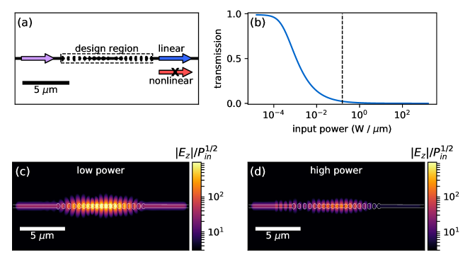
We now apply the general formalism as discussed above to the optimization of nonlinear optical systems. Since the formalism is applicable to linear optical systems as well, for illustration purposes here we use it to treat both the linear and the nonlinear cases, in order to highlight aspects that are unique to nonlinear systems. A schematic outlining the two cases is presented in Fig. 1. For a linear system, Maxwell’s equations for the steady-state at a frequency may be written as
| (9) |
where is the electric field, is the electric current source, is the relative dielectric permittivity, and we have assumed relative permeability everywhere. Compactly, and to make connection to the general formalism in the previous section, this can be written in matrix form as
| (10) |
where is a linear operator, vectors and now contain the electric fields and the relative permittivity, respectively, and is a vector proportional to the current source. The design parameters in this case is the permittivity distribution . Eq. (10) can be solved to obtain the electric fields , as diagrammed by Fig. 1(a).
We assume an objective function that depends on the field solution to eq. (10) and we take the linear relative permittivity distribution as the set of design variables. Because and for the linear system, from eq. (7), the adjoint field may be written simply as the solution to the equation
| (11) |
as shown in Fig. 1(b). For a reciprocal system, , thus the original and the adjoint fields are solutions to the same linear problem but with different source terms. Note that the source for the adjoint field, depends on both the objective function and the original solution.
Once the adjoint field is computed, the gradient of the objective function with respect to the permittivity distribution is given, through eq. (8), by
| (12) | ||||
| (13) |
Having reviewed the adjoint formalism for linear optical systems we now consider nonlinear optical systems. As an example, we introduce Kerr nonlinearity into the system Boyd (2008), which corresponds to an intensity-dependent permittivity
| (14) |
where is the nonlinear susceptibility distribution. Other types of nonlinear terms can also be treated with the formalism outlined above. Replacing in Eq. (9) with in Eq. (14), our system is then described by the equation:
| (15) |
where . Here, is element-wise vector multiplication and represents a diagonal matrix with vector on the main diagonal. The vector corresponds to the term and . Again, for concreteness, the design parameters correspond to the permittivity . The solution to this problem is diagrammed in Fig. 1(c).
From eq. (7) we may now compute the partial derivatives of with respect to the electric fields , which is needed to construct the adjoint problem.
| (16) | ||||
| (17) |
With this, we then express the adjoint field as a solution to the linear system
| (18) |
which is diagrammed in Fig. 1(d).
For a nonlinear system, to obtain the field , one will need to solve a nonlinear equation (e.g. eq. (15)). However, we emphasize that the adjoint problem, as required to determine the derivative of the objective function, is a linear problem. The size of the adjoint problem is twice as large as the corresponding linear problem of Eq. (10), but it is of a similar form, with the source dependent upon the solution .
Once the adjoint field is computed, the gradient is evaluated from eq. (13) as in the linear case. Here for simplicity we do not assume any explicit dependence of the nonlinearity on the design variable. However, the formalism is straightforward to extend to that case, as explained in the Supplementary Information.
III Inverse Design of Optical Switches
We now demonstrate the use of this nonlinear adjoint formalism to inverse design optical switches with desired power-dependent performance characteristics. In Figs. 2 and 3, we show the optimization procedures and performance characteristics of a 1 1 and 1 2 port device, respectively. The operating frequency for both devices correspond to a free-space wavelength of 2m.
For each device, we seek to maximize the corresponding objective function with respect to the permittivity distribution within a fixed design region. To perform the numerical optimization of the structure, we use the finite-difference frequency-domain method (FDFD) Shin and Fan (2012), where the fields and operators of Eq. (9) are spatially discretized using a Yee lattice Yee (1966). For simplicity, we restrict our study to two-dimensional structures (i.e. structures with infinite extent in the third dimension), and transverse-magnetic polarization, which has only non-zero out-of-plane electric field components. In the optimization process, we start with an initial relative permittivity in the design region. We solve the electric field distribution in the structure by solving the nonlinear equation (eq. (15)). Then, we compute the gradient of with respect to the relative permittivity distribution in this region using eq. (13). With the gradient information, we perform updates of the design variables using the limited-memory BFGS Byrd et al. (1995) algorithm, although a simple gradient ascent algorithm would also suffice. This procedure is repeated until convergence on a final structure.
We choose optimization parameters corresponding to a device made from chalcogenide glass (Al2S3), which exhibits a strong response and high damage threshold White and Monro (2011); Lamont et al. (2008); Boyd (2008). During the optimization, the relative permittivity was constrained to lie between (air) and (Al2S3). We further assume that the materials exhibit nonlinearity only within the design regions outlined in Fig. 2(a) and 3(a).
To create a more realistic final structure, the strength of the nonlinear susceptibility was assumed to be proportional to the ”density” of material, , defined as
| (19) |
where is the permittivity of the material. This assumption ensures that air regions do not exhibit a nonlinear refractive index. Eq. (19) adds an dependence in the nonlinear susceptibility, which is straightforwardly treated in the adjoint method, as discussed in the Supplementary Information. Low-pass spatial filtering and projection techniques Zhou et al. (2015) were applied during optimization to create binarized (air and chalcogenide) final structures with large, smoothed features. Additional details on this are described in the Supplementary Information.
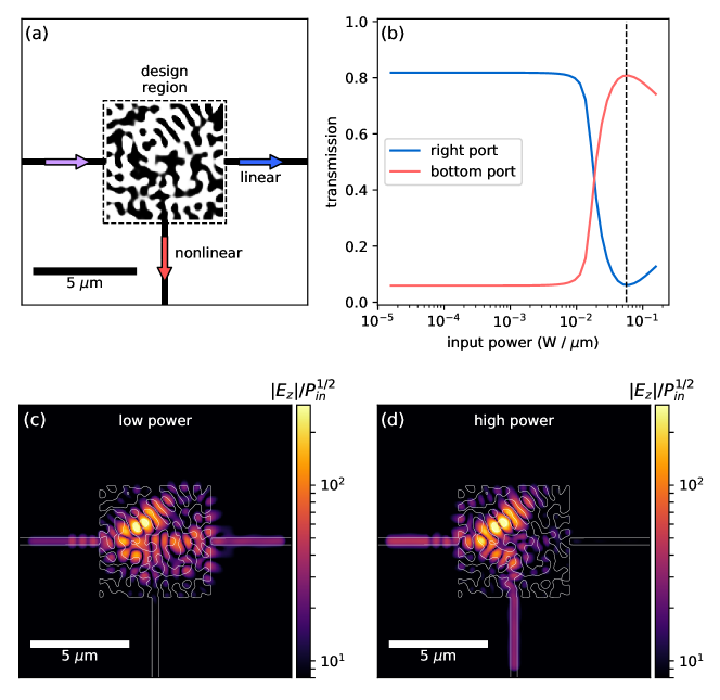
Our first device, as shown in Fig. 2, consists of a waveguide-fed 1 1 port geometry with a central design region. We optimize this design region to maximize power transmission in the linear regime when the incident power is sufficiently low such that the nonlinear terms do not affect the transmission, and minimize transmission in the nonlinear regime when the incident power is at a specific high value such that the nonlinearity plays a significant role. This corresponds to an objective function of the form
| (20) |
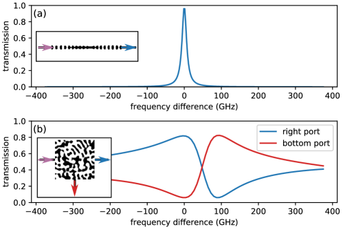
where and are the simulated fields with a low and a high input power, respectively, is the modal profile of the electric field for the waveguide in the output port, and the objective function is normalized such that its maximum value is 1. The optimization setup and the optimized structure are diagrammed in Fig. 2(a). The final structure resembles a resonator between two Bragg mirrors, effectively acting like a bistable switch Soljačić et al. (2002); Yanik et al. (2003). Fig. 2(b) shows the transmission as a function of the input power, and it clearly switches from high to low as the input power increases. This is also illustrated in panels (c)-(d), where we plot the field amplitude distributions in the low-power (high-transmission) regime and in the high-power (low-transmission) regime, respectively. The computed power transmission coefficients for these two panels are 98.2% and 3.1%, respectively. The value of the input power used in the optimization and in panel (d) is shown by a dashed line in panel (b). At this input power, the device exhibits a maximum nonlinear refractive index shift of , which is below the damage threshold for Al2S3 using sub-nanosecond pulses Chorel et al. (2018) (see Supplementary Information). The transmission spectrum of this structure gives a resonance peak with a full-width at half maximum of 38GHz (see Supplementary Information). In the Supplementary Information, we also list the specific optimization parameters, and show the value of the objective function during the optimization process. Reaching the final optimized structure shown in Fig. 2 required the evaluation of 2000 structures, but a reasonably high-performing structure is already reached after only a few hundred iterations.
We also use the same technique for the inverse design of a 1 2 port switch where light is guided to the right port in the linear regime and to the bottom port in the nonlinear regime. To achieve this design, we define the objective function as
| (21) | ||||
where and denote the mode profiles of the waveguides in the right and bottom ports, respectively. These are normalized such that the objective function has a maximum value of 1 for a perfect switching operation. The setup of the optimization problem and the final design are diagrammed in Fig. 3(a). We note that the device displays a non-intuitive geometry while retaining large features and good binarization.
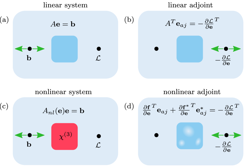
In Fig. 3(b), we plot the transmission through the right and through the bottom ports as a function of input power. This clearly shows the switching of power from the right port to the bottom port in the linear and nonlinear regimes, respectively. Specifically, in the linear regime, the device has a power transmission of 81.8% and 5.9% to the right and bottom ports, respectively, while in the nonlinear regime, at the input power marked by the dashed line in Fig. 3(b), these values are 6.1% and 80.8%, respectively. The electric field amplitudes for linear and nonlinear regimes are displayed in 3(c)-(d). The operational bandwidth for this device is approximately 90 GHz (see Supplementary Information). The device exhibits a maximum nonlinear refractive index shift of , which is also below the acceptable damage threshold for Al2S3 using sub-nanosecond pulses Chorel et al. (2018). A full list of optimization parameters and a plot of the objective function vs. iteration number is shown in the Supplementary Information.
IV Discussion
We have presented an extension to the adjoint variable method applied to the optimization of an electromagnetic system with Kerr nonlinearity. Our approach can be straightforwardly applied to other types of nonlinearities which do not mix frequencies, such as saturable gain or absorption. Moreover, the methods here should be straightforwardly generalizable to treat nonlinear problems involving frequency mixing. For example, one can imagine implementing a similar adjoint method in combination with the multi-frequency finite-difference frequency-domain implementations for nonlinear wave interactions Shi et al. (2016).
In addition to the design of optical switches, our formalism may prove useful for many other interesting problems in nonlinear photonics. For example, one could apply our approach to design nonlinear elements in optical neural networks Shen et al. (2017) with specific forms of activation functions. Another interesting application is power regulation in photonic networks. For example, as photonic networks for laser-driven particle accelerators Hughes et al. (2018a) must be able to handle large input powers, it may be of interest to use our approach to design compact optical limiters in these networks. For the purposes of exploring these and many other potential applications, we have made publicly available a software package that implements the algorithms discussed here Hughes et al. (2018b).
To summarize this paper, we have developed an adjoint method, which enables gradient optimization of nonlinear photonic devices. Our work broadens the capability of inverse design for producing novel nonlinear devices.
This work is supported by the Gordon and Betty Moore Foundation (GBMF4744); the Swiss National Science Foundation (P300P2_177721); and the Air Force Office of Scientific Research (AFOSR) (FA9550-17-1-0002).
References
- Lalau-Keraly et al. (2013) Christopher M. Lalau-Keraly, Samarth Bhargava, Owen D. Miller, and Eli Yablonovitch, “Adjoint shape optimization applied to electromagnetic design,” Optics Express 21, 21693–21701 (2013).
- Wang et al. (2018) Jiahui Wang, Yu Shi, Tyler Hughes, Zhexin Zhao, and Shanhui Fan, “Adjoint-based optimization of active nanophotonic devices,” Optics Express 26, 3236–3248 (2018).
- Elesin et al. (2012) Y. Elesin, B. S. Lazarov, J. S. Jensen, and O. Sigmund, “Design of robust and efficient photonic switches using topology optimization,” Photonics and Nanostructures - Fundamentals and Applications 10, 153–165 (2012).
- Piggott et al. (2017) Alexander Y. Piggott, Jan Petykiewicz, Logan Su, and Jelena Vučković, “Fabrication-constrained nanophotonic inverse design,” Scientific Reports 7, 1786 (2017).
- Piggott et al. (2015) Alexander Y. Piggott, Jesse Lu, Konstantinos G. Lagoudakis, Jan Petykiewicz, Thomas M. Babinec, and Jelena Vučković, “Inverse design and demonstration of a compact and broadband on-chip wavelength demultiplexer,” Nature Photonics 9, 374–377 (2015).
- Kao et al. (2005) C. Y. Kao, S. Osher, and E. Yablonovitch, “Maximizing band gaps in two-dimensional photonic crystals by using level set methods,” Applied Physics B 81, 235–244 (2005).
- Hughes et al. (2017) Tyler Hughes, Georgios Veronis, Kent P. Wootton, R. Joel England, and Shanhui Fan, “Method for computationally efficient design of dielectric laser accelerator structures,” Optics Express 25, 15414–15427 (2017).
- Molesky et al. (2018) Sean Molesky, Zin Lin, Alexander Y. Piggott, Weiliang Jin, Jelena Vučković, and Alejandro W. Rodriguez, “Outlook for inverse design in nanophotonics,” arXiv preprint arXiv:1801.06715 (2018), arXiv: 1801.06715.
- Sigmund and Sondergaard Jensen (2003) O. Sigmund and J. Sondergaard Jensen, “Systematic design of phononic band-gap materials and structures by topology optimization,” Philosophical Transactions of the Royal Society A: Mathematical, Physical and Engineering Sciences 361, 1001–1019 (2003).
- Matzen et al. (2011) René Matzen, Jakob S. Jensen, and Ole Sigmund, “Systematic design of slow-light photonic waveguides,” Journal of the Optical Society of America B 28, 2374–2382 (2011).
- Jensen and Sigmund (2005) Jakob S. Jensen and Ole Sigmund, “Topology optimization of photonic crystal structures: a high-bandwidth low-loss T-junction waveguide,” Journal of the Optical Society of America B 22, 1191 (2005).
- Frellsen et al. (2016) Louise F. Frellsen, Yunhong Ding, Ole Sigmund, and Lars H. Frandsen, “Topology optimized mode multiplexing in silicon-on-insulator photonic wire waveguides,” Optics Express 24, 16866–16873 (2016).
- Shen et al. (2015) Bing Shen, Peng Wang, Randy Polson, and Rajesh Menon, “An integrated-nanophotonics polarization beamsplitter with 2.4 2.4 m footprint,” Nature Photonics 9, 378–382 (2015).
- Shen et al. (2003) Linfang Shen, Zhuo Ye, and Sailing He, “Design of two-dimensional photonic crystals with large absolute band gaps using a genetic algorithm,” Physical Review B 68, 035109 (2003).
- Minkov and Savona (2014) Momchil Minkov and Vincenzo Savona, “Automated optimization of photonic crystal slab cavities.” Scientific reports 4, 5124 (2014).
- Minkov and Savona (2015) Momchil Minkov and Vincenzo Savona, “Wide-band slow light in compact photonic crystal coupled-cavity waveguides,” Optica 2, 631–634 (2015).
- Shi et al. (2018) Yu Shi, Wei Li, Aaswath Raman, and Shanhui Fan, “Optimization of Multilayer Optical Films with a Memetic Algorithm and Mixed Integer Programming,” ACS Photonics 5, 684–691 (2018).
- Veronis et al. (2004) Georgios Veronis, Robert W. Dutton, and Shanhui Fan, “Method for sensitivity analysis of photonic crystal devices,” Optics Letters 29, 2288–2290 (2004).
- Giles and Pierce (2000) Michael B Giles and Niles A Pierce, “An introduction to the adjoint approach to design,” Flow, turbulence and combustion 65, 393–415 (2000).
- Yamashita et al. (2015) Daiki Yamashita, Yasushi Takahashi, Takashi Asano, and Susumu Noda, “Raman shift and strain effect in high-Q photonic crystal silicon nanocavity,” Optics Express 23, 3951 (2015).
- Okawachi et al. (2011) Yoshitomo Okawachi, Kasturi Saha, Jacob S. Levy, Y. Henry Wen, Michal Lipson, and Alexander L. Gaeta, “Octave-spanning frequency comb generation in a silicon nitride chip,” Optics Letters 36, 3398 (2011).
- Moon et al. (1997) Joong Ho Moon, Jin Ho Kim, Ki-jeong Kim, Tai-Hee Kang, Bongsoo Kim, Chan-Ho Kim, Jong Hoon Hahn, and Joon Won Park, “Absolute Surface Density of the Amine Group of the Aminosilylated Thin Layers: Ultraviolet-Visible Spectroscopy, Second Harmonic Generation, and Synchrotron-Radiation Photoelectron Spectroscopy Study,” Langmuir 13, 4305–4310 (1997).
- Khoram et al. (2018) Erfan Khoram, Ang Chen, Dianjing Liu, Qiqi Wang, and Zongfu Yu, “Stochastic optimization of nonlinear nanophotonic media for artificial neural inference,” arXiv preprint arXiv:1810.07815 (2018).
- Guo et al. (2016) Xiang Guo, Chang-Ling Zou, Hojoong Jung, and Hong X. Tang, “On-Chip Strong Coupling and Efficient Frequency Conversion between Telecom and Visible Optical Modes,” Physical Review Letters 117 (2016), 10.1103/PhysRevLett.117.123902.
- Lin et al. (2016) Zin Lin, Xiangdong Liang, Marko Lončar, Steven G. Johnson, and Alejandro W. Rodriguez, “Cavity-enhanced second-harmonic generation via nonlinear-overlap optimization,” Optica 3, 233 (2016).
- Lin et al. (2017) Zin Lin, Marko Lončar, and Alejandro W. Rodriguez, “Topology optimization of multi-track ring resonators and 2d microcavities for nonlinear frequency conversion,” Optics Letters 42, 2818 (2017).
- Bravo-Abad et al. (2007) Jorge Bravo-Abad, Alejandro Rodriguez, Peter Bermel, Steven G. Johnson, John D. Joannopoulos, and Marin Soljačić, “Enhanced nonlinear optics in photonic-crystal microcavities,” Optics Express 15, 16161–16176 (2007).
- Strang (2007) Gilbert Strang, Computational Science and Engineering (Wellesley-Cambridge Press, 2007) chapter 8.
- Press et al. (2007) William H Press, Saul A Teukolsky, William T Vetterling, and Brian P Flannery, Numerical recipes 3rd edition: The art of scientific computing (Cambridge university press, 2007).
- Boyd (2008) Robert W. Boyd, Nonlinear Optics (Academic Press, 2008).
- Shin and Fan (2012) Wonseok Shin and Shanhui Fan, “Choice of the perfectly matched layer boundary condition for frequency-domain maxwell’s equations solvers,” Journal of Computational Physics 231, 3406–3431 (2012).
- Yee (1966) Kane Yee, “Numerical solution of initial boundary value problems involving maxwell’s equations in isotropic media,” IEEE Transactions on antennas and propagation 14, 302–307 (1966).
- Byrd et al. (1995) Richard H Byrd, Peihuang Lu, Jorge Nocedal, and Ciyou Zhu, “A limited memory algorithm for bound constrained optimization,” SIAM Journal on Scientific Computing 16, 1190–1208 (1995).
- White and Monro (2011) Richard T. White and Tanya M. Monro, “Cascaded Raman shifting of high-peak-power nanosecond pulses in as2s3 and as2se3 optical fibers,” Optics Letters 36, 2351 (2011).
- Lamont et al. (2008) Michael R. Lamont, Barry Luther-Davies, Duk-Yong Choi, Steve Madden, and Benjamin J. Eggleton, “Supercontinuum generation in dispersion engineered highly nonlinear ( w/m) as2s3 chalcogenide planar waveguide,” Optics Express 16, 14938 (2008).
- Zhou et al. (2015) Mingdong Zhou, Boyan S Lazarov, Fengwen Wang, and Ole Sigmund, “Minimum length scale in topology optimization by geometric constraints,” Computer Methods in Applied Mechanics and Engineering 293, 266–282 (2015).
- Soljačić et al. (2002) Marin Soljačić, Mihai Ibanescu, Steven G. Johnson, Yoel Fink, and J. D. Joannopoulos, “Optimal bistable switching in nonlinear photonic crystals,” Phys. Rev. E 66, 055601 (2002).
- Yanik et al. (2003) Mehmet Fatih Yanik, Shanhui Fan, Marin Soljačić, and J. D. Joannopoulos, “All-optical transistor action with bistable switching in a photonic crystal cross-waveguide geometry,” Optics Letters 28, 2506 (2003).
- Chorel et al. (2018) Marine Chorel, Thomas Lanternier, Eric Lavastre, Nicolas Bonod, Bruno Bousquet, and Jérôme Néauport, “Robust optimization of the laser induced damage threshold of dielectric mirrors for high power lasers,” Optics express 26, 11764–11774 (2018).
- Shi et al. (2016) Yu Shi, Wonseok Shin, and Shanhui Fan, “Multi-frequency finite-difference frequency-domain algorithm for active nanophotonic device simulations,” Optica 3, 1256–1259 (2016).
- Shen et al. (2017) Yichen Shen, Nicholas C Harris, Scott Skirlo, Mihika Prabhu, Tom Baehr-Jones, Michael Hochberg, Xin Sun, Shijie Zhao, Hugo Larochelle, Dirk Englund, and Marin Soljačić, “Deep learning with coherent nanophotonic circuits,” Nature Photonics 11, 441 (2017).
- Hughes et al. (2018a) Tyler W. Hughes, Si Tan, Zhexin Zhao, Neil V. Sapra, Kenneth J. Leedle, Huiyang Deng, Yu Miao, Dylan S. Black, Olav Solgaard, James S. Harris, Jelena Vuckovic, Robert L. Byer, Shanhui Fan, R. Joel England, Yun Jo Lee, and Minghao Qi, “On-chip laser-power delivery system for dielectric laser accelerators,” Physical Review Applied 9, 054017 (2018a).
- Hughes et al. (2018b) Tyler W Hughes, Momchil Minkov, and Ian A D Williamson, “Angler – an adjoint nonliner gradient open-source package,” https://github.com/fancompute/angler (2018b).
Supplementary Information
V Optimization Details
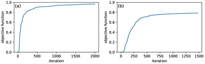
Table S1 contains the parameters used in the inverse design demonstrations of Fig. 2 and Fig. 3 of the main text. The values of the objective function vs. iteration are shown in Fig. S1 for both the 2-port and 3-port devices.
| parameter | symbol | value (2-port) | value (3-port) | units |
|---|---|---|---|---|
| max relative permittivity | 5.95 | 5.95 | - | |
| nonlinear susceptibility | m2 V-2 | |||
| input power | 157 | 57 | mW/m | |
| free space wavelength | 2 | 2 | m | |
| design region length | 10 | 6 | ||
| design region height | 1.6 | 6 | ||
| waveguide width | 300 | 300 | nm | |
| grid size | g | 40 | 40 | nm |
| low-pass filter feature size | R | 160 | 200 | nm |
| projection strength | 100 | 500 | - | |
| projection mid-point | 0.5 | 0.5 | - |
.
VI Permittivity-dependent Nonlinear Susceptibility
In the inverse design demonstration of the main text, we made the assumption that the nonlinear susceptibility distribution was proportional to the density of material in the design region. Here we will derive the form of the adjoint sensitivity with this modification.
With our assumption, the nonlinear susceptibility vector may be written in terms of the scalar magnitude of the nonlinear susceptibility and the relative permittivity vector explicitly as
| (S1) |
where is a vector of all ones and is the maximum relative permittivity allowed in the optimization, corresponding to the material relative permittivity.
When choosing to relative permittivity distribution as the set of design variables, , the nonlinear adjoint problem requires the calculation of the partial derivatives , , and . When choosing the form of from eq. (S1), the partial derivatives and are the same as derived in the main text. However, the term takes on a more complicated form given by
| (S2) | ||||
| (S3) | ||||
| (S4) |
where we make use of the fact that , where is the Kronecker delta.
Thus, while the adjoint field will have the same form as in the main text, when computing the sensitivity as in eq. (8) in the main text, one must insert the form of from eq. (S4). This is in contrast to the usual case where the nonlinear susceptibility is fixed, .
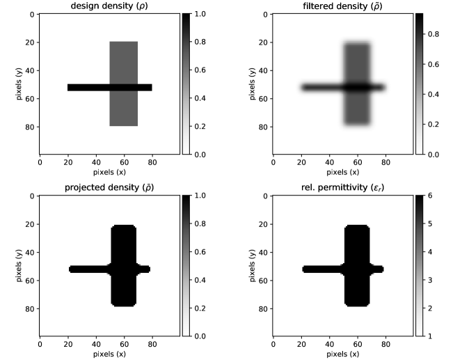
VII Maintaining minimum feature size and binarization
To create realistic devices with sufficiently large minimum feature sizes and binarized permittivity distributions, we employed filtering and projection schemes during our optimization. These schemes are discussed in great detail in Zhou et al. (2015) and related works.
Rather than updating the permittivity distribution directly, one may instead choose to update a design density , which varies between 0 and 1 within the design region. To create a structure with larger feature sizes, a low pass filter can be applied to to created a filtered density, labelled :
| (S5) |
where denotes the design region, and is the spatial filter, defined for a feature size of as
| (S6) |
with being the distance between points and . This defines a low-pass spatial filter on with the effect of smoothing out features with length scale below .
Now, for binarization of the structure, a projection scheme is used to recreate the final permittivity from the filtered density. For this we define as the projected density, which is created from as
| (S7) |
Here, is a parameter between 0 and 1 that controls the mid-point of the projection, typically 0.5, and controls the strength of the projection, typically around 100.
The relative permittivity can then be determined from as
| (S8) |
where is the maximum permittivity.
The effect of these filtering and the binarization techniques on a sample permittivity set is illustrated in Fig. S2. In the optimizations of the main text, these techniques were performed only within the design region and required minimal modifications to the adjoint sensitivity. The determination of , , and were required to compute the derivatives of the objective function with respect to the underlying . For more details, see the software package accompanying this work Hughes et al. (2018b).
VIII Nonlinear Index Shift
Here we estimate the maximum nonlinear index shift of chalcogenide (Al2S3) materials. Based on Boyd (2008); Lamont et al. (2008); White and Monro (2011), Al2S3 has a nonlinear index () between and cm2/W. From Chorel et al. (2018), the damage threshold is 2.5 J/cm2. At a pulse duration of 100 ps, this damage threshold corresponds to W/cm2. Together with the nonlinear refractive index, the maximum refractive index shift sustainable by the material is approximately
| (S9) |
with a corresponding pulse bandwidth (for a bandwidth-limited Gaussian pulse) of GHz. Our final structures exhibit maximum refractive index shifts below and their objective functions have FWHM bandwidths above 10 GHz. This suggests that they should exhibit their desired switching effects without damage using pulse durations on the order of 100 ps and input powers on the order of 100 mW/m.
IX Transmission Spectra
The transmission vs. frequency for the two devices in the main text is shown in Fig. S3 in the linear regime.