Large-Area, Low-Noise, High Speed, Photodiode-Based
Fluorescence Detectors with Fast Overdrive Recovery
S. Bickman, D. DeMille
Yale University, Physics Department, PO Box 208120, SPL 23, New Haven, CT, 06520
Abstract
Two large-area, low noise, high speed fluorescence detectors have been built. One detector consists of a photodiode with an area of 28 mm x 28 mm and a low noise transimpedance amplifier. This detector has a input light-equivalent spectral noise density of less than 3 pW/, can recover from a large scattered light pulse within 10 s, and has a bandwidth of at least 900 kHz. The second detector consists of a 16 mm diameter avalanche photodiode and a low-noise transimpedance amplifier. This detector has an input light-equivalent spectral noise density of 0.08 pW/, also can recover from a large scattered light pulse within 10 s, and has a bandwidth of 1 MHz.
I Introduction
Two large-area, high speed, photodiode-based fluorescence detectors have been built to detect fluorescence from molecules excited via a pulsed laser system. Both detectors have a large area to allow for collection of light from a large solid angle and are fast to allow for good time resolution of the fluorescence. Since the high intensity of pulsed laser systems inevitably scatters a significant number of photons into the detector, both detectors are designed to quickly recover from a large pulse of light that would otherwise saturate the detector for the duration of the fluorescence signal.
While photomultiplier tubes (PMTs) can also be used to measure fluorescence after excitation with a pulsed laser, photodiodes and avalanche photodiodes (APDs) have several advantages. Photodiodes typically have a much higher quantum efficiency (q.e.) than PMTs. For example, at 550 nm (where this detector is used) PMTs have q.e.20% while Silicon PIN photodiodes have q.e.85% and the APD used in this detector has q.e.80%. Furthermore, photodiodes have a more linear response to light intensity than PMTs and can withstand higher sustained fluxes.
One of these detectors will be used in an experiment that intends to improve the sensitivity to an electron electric dipole moment (EDM)[1]. The experiment detects small energy shifts in an excited state of PbO that would result from a non-zero EDM. The energy shifts are measured with quantum beat spectroscopy [2], which in this case appears as a sinusoidal modulation at 200-500 kHz superimposed on an exponential decay due to the spontaneous emission of an excited state of PbO[3]. In order to maximize the solid angle of detection, large area photodiodes or APDs are used. The Hamamatsu S3584-08 silicon PIN photodiode has an area of 28 mm x 28 mm and the Advanced Photonix 630-70-73-500 APD has a diameter of 16 mm.
While PMTs have an intrinsic nearly noise-free gain stage, PIN photodiodes do not and the gain in APDs is smaller than the desired gain. Thus, low noise transimpedance preamplifiers are necessary for the photodiode-based detectors. There were three requirements for the design of the preamplifiers in our experiment. First, the intrinsic noise of the amplifiers must be less than the anticipated shot noise, so that the amplifier noise will not significantly contribute to the overall noise on the detected signal. Second, since the photodiode or APD is exposed to a large pulse of scattered light from the excitation laser, the preamplifier must be able to recover quickly from such a pulse. We specifically require recovery in 10 s, since the excited state has a lifetime of 50 s under the current conditions. Finally, to allow for unattenuated detection of quantum beats at 500 kHz, the preamplifier must have a bandwidth of 1 MHz.
II Low noise amplification

The noise of a transimpedance amplifier can be modelled as shown in figure 1[4]. All noise components will be calculated at the output of the transimpedance amplifier. A real photodiode can be modelled as an ideal photodiode in parallel with a capacitor and a shunt resistor , plus resistance in series with the other components. and are the feedback capacitance and resistance and is the amplifier input capacitance.
All of the resistances in this model have intrinsic Johnson noise. The voltage noise spectral density across a resistance is given by . At the output of the amplifier, the Johnson noise of contributes
| (1) |
where and . At the output of the amplifier, the Johnson noise from gives
| (2) |
and the Johnson noise from gives
| (3) |
In addition to Johnson noise, we must consider the voltage and current noise at the input of the amplifier. At the output of the amplifier, the input voltage noise of the amplifier contributes
| (4) |
The input current noise , at the output of the amplifier, gives
| (5) |
In this application, it is necessary to keep the total electronic noise less than the shot noise. The expected signal size is photoelectrons, in an exponential decay with a time constant of . For a signal current , the current noise spectral density at the input of the detector is
| (6) |
Here is the intrinsic gain of the detector; =1 for a PIN photodiode, while =200 for the APD used here. Also, is an additional noise factor associated with the gain process. For the PIN photodiode, =1, while for an APD [5]. In the case of the APD used here, this additional noise was measured as indistinguishable from F=2. At the output of the amplifier, this becomes
| (7) |
A PIN Photodiode
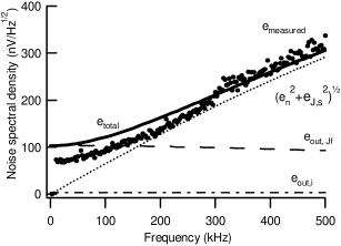
In the photodiode transimpedance amplifier, the feedback resistor was chosen to be 600 k. In this case, the shot noise on the signal (at low frequencies) is =0.3 V (also at low frequencies) which is larger than the Johnson noise of the feedback resistor for the first 100 s of the decay since =0.1 V when . Having chosen =600 k, it is possible to make some estimates of which noise terms are important. The Hamamatsu S3584-08 photodiode used to detect the signals has a capacitance pF when reverse biased and resistances 5 G and . is approximately 0.3 pF in order to maintain the desired bandwidth. With these values, the significant noise sources are , , and , which all contribute on the order of V/ at the output. At high frequencies, , so it is necessary to keep nV/. and contribute very little to the noise (see figure 2).
In order to control the input voltage and current noise of the amplifier at the desired level, it is necessary to use a low noise JFET as the the input stage of the amplifier. Most low-noise operational amplifiers have an input voltage spectral noise which is too high for this application. Each of the IF9030 JFETs used here has = 0.5 nV/. These JFETs do not have enough gain to achieve the desired transimpedance gain of , so this stage is followed by an operational amplifier[6]. The JFET input stage provides a low-noise amplification stage before the noisier second stage op-amp. The gain of the JFET amplifier is sufficiently large that the input noise of the op-amp is negligible.
The input voltage noise can be further reduced by putting JFETs in parallel resulting in a combined noise of =. In principle, many JFETs can be used to improve the noise of the amplifier, but in practice there are two limitations. The ultra-low noise JFETs used here have a significant gate-source capacitance . Since the noise at the output of the amplifier at high frequencies scales as , the number of parallel JFETs has an optimum value [7]. Also, since is of the same order as , there is little improvement to the noise once .
Requirements for the second stage of amplification were also stringent. At high frequencies the closed-loop voltage gain of the entire preamplifier is . However, the voltage gain of the JFET front-end is only , determined by the JFET transconductance of S and the drain resistance of k. The Miller effect significantly reduces the gain of the JFET stage at high frequencies, so a cascode configuration was used to reduce this effect[8]. Even with the cascode, the second stage amplifier must have a high gain and wide bandwidth so that the open loop gain is large enough. We use the Analog Devices AD797, which which has a gain bandwidth product GBW of 110 MHz, and has nV/. In addition to the high GBW of the AD797, this op-amp was chosen for its fast recovery from overdrive, which allows it to quickly recovery from the scattered light pulse.
B APD
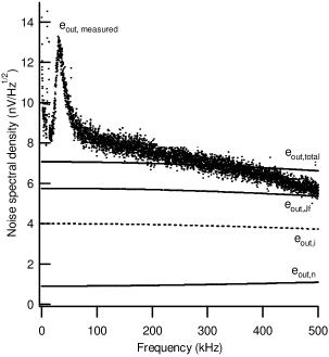
The noise design of the transimpedance amplifier for the APD is much less stringent since the bias voltage is chosen so the APD gain G200. The shot noise at the output of the APD is thus larger than the noise in the PIN photodiode. We choose =2 k in the transimpedance amplifier for the APD, resulting in shot noise at the output of the amplifier . Having chosen and knowing that =140 pF for this APD, it is possible to make some estimates of which noise terms are significant. We find that and have insignificant noise contributions. Since the noise requirements are much less strict for this amplifier, no front-end JFET was used. Instead the transimpedance amplifier is made from a single op-amp, the AD797, which has again been chosen for its high GBW and fast overdrive recovery time. The AD797 has nV/ and pA/. At the output of the transimpedance amplifier, 5.8 nV/. The voltage noise is almost insignificant since 1.3 nV/. The current noise is the largest expected noise contribution at 3.7 nV/. The various noise contributions along with the measured noise are shown in figure 3.
There are two other noise sources that are significant with the APD detector, but not the photodiode detector. The first is the shot noise in the dark current of the APD . In this case, this shot noise is negligible compared to the shot noise on the expected signal. The second is the noise on the bias voltage for the APD. The photodiode bias voltage was supplied by batteries, but the necessary high bias voltage for the APD makes it difficult to supply with batteries. A high voltage power supply was used and filtered to provide acceptable noise characteristics for the APD detector.
III Recovery time from scattered light pulse
Many experiments observe the fluorescence from atoms or molecules that are excited with a pulsed laser. These high intensity beams scatter photons into the detector causing a large, but temporally short burst of photoelectrons. In many cases, this scattered light pulse is several orders of magnitude larger than the expected signal size, and can easily saturate the detector system. In our case, the transimpedance amplifier must be able to recover from this scattered light pulse, which is injected in a 5 ns duration, quickly in order to observe the spontaneous fluorescence. We define the recovery time as the time that it takes the amplifier to ring down to 1/e of the saturated value.
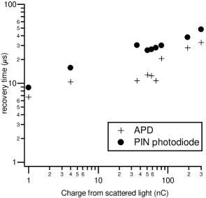
The recovery time of the amplifier depends on the size of the scattered light pulse. For this experiment, it was necessary to choose optical filters that reduced the signal size, but also reduced the scattered light. The two filtering options we considered allowed for a scattered light pulse that injected a charge of either 220 nC or 1.5 nC at the expense of a factor of 3 smaller desirable signal in the latter case. The photodiode and APD both took more than 50 s to recover from the 220 nC pulse and s to recover from the 1.5 nC pulse. The recovery time as a function of injected charge from scattered light is shown in figure 4 for both detectors.
Three changes were made to the design of the transimpedance amplifiers to improve the recovery time. First, clamping diodes were placed between the output of the photodiode or APD and ground to shunt large input light signals to ground. Small signal and Schottky diodes were used and both kinds were chosen for their low capacitance so as not to significantly contribute to . The Schottky diodes were chosen for their low forward voltage drop, and the small signal diodes were chosen for their higher current ratings. These diodes are placed in opposite directions to damp additional electronic ringing due to the scattered light pulse.
The second and third changes were only applied to the photodiode amplifier. Here, diodes were placed in the feedback loop to allow for a low resistance path when the amplifier was saturated. These diodes were not necessary in the APD amplifier because is much smaller. The cascode in the JFET stage improved the recovery time by increasing the bandwidth of this stage of the amplifier.
Preliminary circuit designs used two additional methods of improving the recovery time, but these methods were not successful enough to be used in the final design. The first method was to add a power booster in the feedback loop for the photodiode detector. This power booster was able to source more current through the diodes in the feedback loop of this detector in an attempt to shorten the recovery time. In this application, it was difficult to implement the power booster as it made the feedback traces larger, and difficult to minimize. The second method was to add an additional photodiode at the input of the transimpedance amplifier with opposite orientation to the detecting photodiode. A laser diode shone into the additional diode providing some charge cancellation during the scattered light pulse. However, the improvement in recovery time was found to be negligible.


IV Frequency Response
In order to achieve the desired bandwidth of 1 MHz with a feedback resistor of 600 k in the PIN photodiode transimpedance amplifier, it is necessary to keep the feedback capacitance less than 0.26 pF. Since the diodes used to decrease the scattered light recovery time have a combined capacitance of 0.2 pF, it is necessary to keep all other possible capacitances extremely low. For this reason, three 200 k resistors were used in series to create the feedback resistor. Additionally, the circuit board was designed to keep the traces relating to the components in the feedback loop as short as possible by placing feedback components on the opposite side of the circuit board from the amplifying components. Ground planes were placed on all available surfaces on the circuit board and two inner layers of the circuit board were also grounded. The 3dB bandwidth of the circuit was measured as 900 kHz, implying 0.3 pF (see figure 5).
The smaller in the APD amplifier makes it much less sensitive to frequency limitations and this amplifier could be made to have a bandwidth of at least 10 MHz if necessary. Our present APD detector has a bandwidth of 1 MHz.
V Final Design
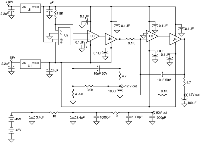
The final design incorporated all of the elements discussed above. The circuit diagram for the PIN photodiode detector is shown in figure 6. The circuit boards were designed with great care to minimize the path lengths at the input of the amplifier. These short paths reduce capacitive effects and noise pickup from other sources. Surface mount components were used wherever possible to reduce lead size. All cables leading to or from the circuit board are made of coaxial cable. The power supplies for the photodiode detector were also constructed to minimize noise. The design of the power supplies is shown in figure 7.
The final design for the APD detector is shown in figure 8. The power supply for the bias voltage was filtered to remove high frequency noise components.

VI Summary
The large-area (7.8 cm2) PIN photodiode detector described here has an input light-equivalent noise of less than 3 pW/ at a wavelength of 550 nm, can recover in 10 s from large scattered light pulses that rapidly inject 1.5 nC of charge, and has a bandwidth of more than 900 kHz. The noise was minimized by using a large feedback resistance to minimize Johnson noise, JFETs as the first stage of the amplifier to , and low noise power supplies. The recovery time from the scattered light was reduced by using clamping diodes on the input and in the feedback, and with a cascode configuration on the JFET front end. The bandwidth was achieved by minimizing all capacitances.
The final design for the large-area (2.0 cm2) APD detector has an input light-equivalent noise of 0.08 pW/, can recovery quickly from large scattered light pulses and easily has a bandwidth of 1MHz. Quantum beats were observed with this APD detector; however, the signals in the current experimental configuration are much smaller than ultimately anticipated. In figure 9, simulated signals at the anticipated level of 0.6 A, with quantum beats at 500 kHz, are shown as measured with the APD. These signals were simulated with an LED driven by an arbitrary waveform generator programmed to simulate the beat signal. The trace in figure 9 includes scattered light equivalent to 1.5 nC of charge injection.

VII Acknowledgements
We are grateful for the support of NSF Grant No. PHY0244927, and the David and Lucile Packard Foundation. We thank David Kawall and Valmiki Prasad for helpful discussions.
References
- [1] D. Kawall, F. Bay, S. Bickman, Y. Jiang, and D. DeMille Phys. Rev. Lett. 92, 133007 (2004)
- [2] S. Haroche in High-Resolution Laser Spectroscopy edited by K. Shimoda (Springer-Verlag, Berlin, 1976), Chap. 7, pp 253-313.
- [3] D. DeMille, F. Bay, S. Bickman, D. Kawall, D. Krause, Jr., S. E. Maxwell, and L. R. Hunter, Phys. Rev. A 61, 052507 (2000).
- [4] J. Graeme, Photodiode Amplifiers: Op-Amp Solutions. McGraw-Hill, New York 1996.
- [5] Ammon Yariv. Optical Electronics, Third Edition, CBS College Publishing, USA (1985).
- [6] D.Yvon, A. Cummings, W. Stockwell, P. Barnes, C. Stanton, B. Sadoulet, T. Schutt, C. Stubbs, Nucl. Instr. and Meth. in Phys. Res. A 368 (1996) 778-788.
- [7] Paul Horowitz, and Winfield Hill. The Art of Electronics, Second Edition, Cambridge University Press, USA (1998).
- [8] Steven R. Jefferts, and F.L. Walls. Rev. Sci. Instru. 60 (1989) 1194-1196.